Continue to Site

Welcome to EDAboard.com

Welcome to our site! EDAboard.com is an international Electronics Discussion Forum focused on EDA software, circuits, schematics, books, theory, papers, asic, pld, 8051, DSP, Network, RF, Analog Design, PCB, Service Manuals... and a whole lot more! To participate you need to register. Registration is free. Click here to register now.

Lowpass Filter: How to layout lumped elements?

Status
Not open for further replies.

ferdem

Full Member level 2
Joined
Oct 18, 2008
Messages
135
Helped
31
Reputation
62
Reaction score
35
Trophy points
1,308
Location
Türkiye
Activity points
2,866
Hi friends, I want to design a lowpass filter with lumped elements. I have no specs to meet, my goal is just study on lumped element filters. Operating range is DC to 1GHz.
I have tried for fcut=160 Mhz simulated in AWR(schematic only)
**broken link removed**
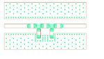
and made a quick layout:
**broken link removed**
then I realized it.
As you guess, network analyser measurments did not match with simulation results. Sharp edge between passband and stopband got smoother in real circuit and 3db cutoff frequency has shifted to 100 MHz(160MHz intended).

My questions:
1) Which one more suitable, wire wound inductors or chip inductors and what about their Q values?
2) How do you determine orientation of components and spaces between them, is it a good habit to place inductors perpendicular to trace?
3) Would you use an EM simulator for this design?
I'm aware of planar em simulators, are there simulators/tools modeling em behavior of lumped elements, which one do u recommend?
I have applied for Sonnet evaluation to use with AWR, is this a enough combination to simulate above design?
Thank you very much, sincerely.
 

1) Which one more suitable, wire wound inductors or chip inductors and what about their Q values?
The answer will be exactly answered by manufacturer datasheets. Wirewound has generally lower Q. You can also add a series resistor according to the real Q to your circuit to determine it's effect. Good filter calculation tools alsways have this option.

Your filter designed won't be much affected by the Q of good wirewound chip inductors. The most serious disturbance is apparently created by the rather long traces between inductors and stubs at the capacitors. The latter will considerably reduce the stop band attenuation. The "horizontal" L can be reduced by shortening the traces an partly considered in the lumped inductor dimensioning. You can simply add known characteristic L and C according to your trace dimensions to the circuit.

At 100 or 200 MHz, you won't absolutely need an exact EM simulation I think, just a correction of circuit elements.
 

c5 and c6 do not have any via holes to the ground plane on the backside. That is a major no-no. Think of what the currents going thru those capacitors have to go thru to return to the backside!

Also you do not show input/output connectors. They need to be well-attached to that backside groundplane too.

At higher frequencies that length of line between the t junctions and the locations of the capacitors would have a big impact, but you can probably get away with it at 160 MHz. In a future layout, more the two capacitors closer. (for that mater, move the inductors closer to the caps too--that transmission line length alters the effective inductance value).

Rich
 
Last edited by a moderator:

-Download design kits of passive component manufacturers to simulate with realistic models including Q, s-parameters.. etc.
-Use small components as much as possible to decrease parasitic elements... For instance 0402 or 0603
-Layout must be carefully designed so that there shouldn't be any series parasitic inductance or parallel capacitance etc.. Your layout should be corrected with this argument..It's not a good layout..
-If you have EM simulation capability use it in a co-simulation with design kit components..
-use 2 layers board and put vias proper places as much as possible..
Finally... use high quality connectors for realistic results... don't buy cheap shits..
 

Thanks for the answers. Actually c5 and c6 have via holes, whole layout is here:
**broken link removed**
I post realized circuit to show input-output connectors.
**broken link removed**

**broken link removed**

Connectors are box type sma connectors and only bottom side is soldered. Another deficiency pertaining to connections is that there is a small ground free area where the connectors enter the board. Small ground free area is thought for safe soldering but it slightly hurts impedance there(pulls it from 50 to 42-43 ohm). Box type connectors have worked well in my other designs(<1G) and I have examined impedances of microstrip traces and connections in my test boards with TDR device, I have seen that line impedance even in connection area is close to 50 ohm, min 42@connections, max 52 on the line. Grounding or connection may not be perfect but I think the main problem is neither of them.


I have a working lumped element lowpass filter to compare with mine, its cut off frequency is 100MHz. Orders are same, It has 5(2ind+3cap) components, I have 5 components. However, it is laid out almost 3 times larger area than my board and wirewound inductors have been used, they have been placed far from each other and their directions look engineered! Ideas and comments will be welcome, sincerely.

I have just noticed your post, thanks BigBoss. Thanks all for your valuable recommendations.
 

Don't use thermal reliefs for ground connections. instead connect the components directly to the ground...
Especially connector groundings are not properly done on your layout..
Don't put ground pattern very close around filter elements, it will create some fring capacitances between components and ground that are unwanted..it's very important..
 

Attachments

  • Filter.png
    Filter.png
    24.8 KB · Views: 67
Last edited:

Wire wound air coil always has higher Q than chip inductors. Besides, you can easily change the inductor value by spreading or squeezing the coils.
 

you can easily change the inductor value by spreading or squeezing the coils.
Im curious to see how you do with a 0402 or 0603 chip inductor :lol:
 

Status
Not open for further replies.

Part and Inventory Search

Welcome to EDABoard.com

Sponsor

Back
Top