mr bobo
Newbie level 3
Hello experts!
I am newbie here.
I am in the first year of Electronics Engineering. So my Analog Communication teacher gave us an assignment and told us to make the Low Level AM Transmitter. The assignment summary goes as follows
Project summary
The aim is to design, build and test an AM system using a carrier frequency in the
15-25kHz range. The modulating input signal will be an audio waveform in the
range 250Hz – 1.5kHz. The system will consist of a transmitter (modulator) and
receiver (demodulator) along with input and output filters and amplifiers as required.
Only two DC supply voltages are to be used and amplifiers/buffers should be opamp
based (e.g.TL071). A maximum of 4 op-amps can be used in the system
design.
Transmitter: The transmitter will take an input sinusoidal signal with an amplitude of
no more than 200mV and a maximum frequency of 2kHz which will be used to
modulate the amplitude of a sinusoidal carrier wave in the 10-20kHz range. The
carrier frequency will be taken from the signal generator and you should build an
oscillator (e.g. Wien bridge) to provide the modulating signal.
Amplitude modulation should be achieved using a switching modulator based on a
nonlinear device: the performance of switching modulator circuits based on a diode
and a BJT should be compared.
Transmission line: In a real system a transmission line would typically have 50Ohm
impedance. In the project the transmission line will be replaced with a 50Ohm
resistor to provide the impedance between transmitter and receiver.
Receiver: The receiver will be based on an envelope detector circuit with additional
filtering as required to give an output signal which is a replica of the input
modulating signal. The output from the receiver should AC coupled with an
amplitude of at least 200mV when driving a 50Ohm load.
He went on to give me a specific signal frequency of 420hz and the carrier frequency of 21Khz
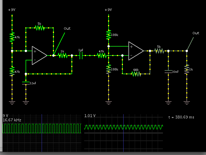
i have managed to look around on the web for some information and i did background research and designed schematic using isis but i have hit the wall beacuse im so confused on how to go further. I have attached a pic of my schematic
i would appreciate it if any one of you expert will help me because i only got 4days to finish the design and start on the testing of the it

Thank you.
I am newbie here.
I am in the first year of Electronics Engineering. So my Analog Communication teacher gave us an assignment and told us to make the Low Level AM Transmitter. The assignment summary goes as follows
Project summary
The aim is to design, build and test an AM system using a carrier frequency in the
15-25kHz range. The modulating input signal will be an audio waveform in the
range 250Hz – 1.5kHz. The system will consist of a transmitter (modulator) and
receiver (demodulator) along with input and output filters and amplifiers as required.
Only two DC supply voltages are to be used and amplifiers/buffers should be opamp
based (e.g.TL071). A maximum of 4 op-amps can be used in the system
design.
Transmitter: The transmitter will take an input sinusoidal signal with an amplitude of
no more than 200mV and a maximum frequency of 2kHz which will be used to
modulate the amplitude of a sinusoidal carrier wave in the 10-20kHz range. The
carrier frequency will be taken from the signal generator and you should build an
oscillator (e.g. Wien bridge) to provide the modulating signal.
Amplitude modulation should be achieved using a switching modulator based on a
nonlinear device: the performance of switching modulator circuits based on a diode
and a BJT should be compared.
Transmission line: In a real system a transmission line would typically have 50Ohm
impedance. In the project the transmission line will be replaced with a 50Ohm
resistor to provide the impedance between transmitter and receiver.
Receiver: The receiver will be based on an envelope detector circuit with additional
filtering as required to give an output signal which is a replica of the input
modulating signal. The output from the receiver should AC coupled with an
amplitude of at least 200mV when driving a 50Ohm load.
He went on to give me a specific signal frequency of 420hz and the carrier frequency of 21Khz
i have managed to look around on the web for some information and i did background research and designed schematic using isis but i have hit the wall beacuse im so confused on how to go further. I have attached a pic of my schematic
i would appreciate it if any one of you expert will help me because i only got 4days to finish the design and start on the testing of the it
Thank you.