Continue to Site

Welcome to EDAboard.com

Welcome to our site! EDAboard.com is an international Electronics Discussion Forum focused on EDA software, circuits, schematics, books, theory, papers, asic, pld, 8051, DSP, Network, RF, Analog Design, PCB, Service Manuals... and a whole lot more! To participate you need to register. Registration is free. Click here to register now.

low current Power On Reset (POR) circuit ?

Status
Not open for further replies.

cmos_ajay

Full Member level 2
Joined
Jan 30, 2007
Messages
126
Helped
0
Reputation
0
Reaction score
0
Trophy points
1,296
Activity points
2,247
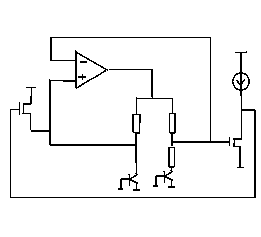
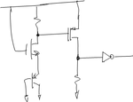
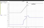
Hello, I need to design a power on reset circuit that consumes only 0.7 micro ampere. Supply voltage VDD can range from 1.4V and above. When the supply is rising and it reaches say 1.2V, the POR signal should go high. Can you suggest any robust architecture for this ? Any schematic or technical document will be of great help. Thanks .
 

What kind of technology are you working on? Also what is the accuracy and hysteresis requirements on the threshold? How high does the VDD go? Is the current spec for the highest VDD or just for some particular VDD?
 

    V

    Points: 2
    Helpful Answer Positive Rating
Hello, I am using a 0.25um CMOS technology. VDD can go upto 2.75V max. and I expect the POR to go high when VDD has reached 1.1V
The current spec. is for the highest VDD (2.75V). Any suggestions ??
 

What kind of accuracy do you require on the POR spec over Process and temperature. Do you have bipolars? I think you would need to make a low voltage reference and then use a comparator. A low voltage reference may be done like the one shown in the paper attached.
 

Attachments

  • Paper.pdf
    261.4 KB · Views: 260
  • Like
Reactions: khite

    khite

    Points: 2
    Helpful Answer Positive Rating
Hello, Thanks for the document. I do have bipolar devices in my library. Typically, I was thinking of using a basic bandgap core with a comparator. I would use a resistively divided VDD for comparison with the bandgap voltage. Trip point variation under process and temperature can be 1.1 to 1.25V.
* It is important that the bandgap voltage arrives at the comparator first and then the divided VDD arrives at the comparator. If not there will be a glitch in the o/p. How do I achieve this correct sequence ?? Thanks.
 

You need to make sure that whatever Bandgap reference you use is stable at a supply much lower than your trip point. Also you need to generate a Bandgap OK signal saying that your bandgap voltage is fine. The way to generate would be to either look at the bandgap voltage or maybe look at the VDD when it crosses 2 thresholds or whatever is the minimum headroom required by your bandgap. Then give a long delay which makes sure in the worst case the bandgap is up and correct after the delay. Gate the final comparator output with this generated Bandgap OK signal.
 

Assume the bandgap voltage is say 0.9V and I need to generate a OK signal. An inverter with vtrip = 0.9V is fine. But if VDD was raised to 2.7V, then the inverter trip point will increase. So this may not be good. "Look at the VDD when it crosses 2 thresholds or whatever is the minimum headroom required by your bandgap" ....Can you explain this with some diagram or maybe more words. My VDD ramp rate can be quite high. Thanks.
 

I would make the bandgap more lower to give more margin. If your bandgap can operate fine with a Vbe and Vth headroom for example the one shown in the paper then you may make a VDD detector something like the one attached.
 

Attachments

  • VDD_detection.png
    VDD_detection.png
    7.6 KB · Views: 182
Thanks for the reply. Why do you need a BJT in the VDD detector that you have drawn ? If temp. increases, then Veb reduces and Vgs (nmos) increases. So Id(nmos) increases. Can you please explain ? Regards.
 

The bjt is there to track with the reference in the paper. Since the headroom required by the circuit in the pauperism roughly vbe+vth hence I have a vibe and a vth stacked in the detector circuit so that it tracks the reference headroom requirement.
 

Hello, I have made the circuit with a bandgap core, a divided VDD and a comparator to be used as the POR. At a fast ramp rate 0 to VDD in 50 us, the bandgap does not settle fast enough. The bandgap o/p rises up, shows an overshoot and then settles to its final steady state value.
Is it appropriate to make the comparison at the comparator when the bandgap is overshooting ?? My feeling is that it is better to wait till the bandgap has settled to its steady state value and then apply the divided VDD (delayed version) to the other input of the comparator so that the comparator circuit makes a proper comparison. Any suggestions are welcome ?? Thanks.
 

The comparison should be made when the bandgap has settled fully. And it would be much easier to ignore the comparator output till the bandgap has settled rather than removing and applying the divided down VDD at the input. As I suggested above you should create a bandgap ok signal which has a built in delay long enough that makes sure that in the worst case or Process, voltage and temperature your bandgap is stable (plus some comparator delay if the comparator is also slow) and then use that bandgap ok signal to gate the comparator output.
 

Hello, Since the VDD is rising too fast ( 0 to 1.4V in 50us ) the bandgap does 'not' settle when VDD = 1.1V. The desired reset threshold voltage is 1.1V. When VDD reaches the reset threshold value of 1.1V, a trigger signal is generated . Then a delay cell is activated by this trigger signal and the POR goes high. Thus the part will be 'released' from reset once the POR o/p goes high. Is there a simple bandgap architecture that can settle good enough at VDD = 1.1 ? Attached is a waveform. Thanks and regards.
 

Attachments

  • bgp_fast.jpg
    bgp_fast.jpg
    194.9 KB · Views: 155

The bandgap doesn't need to settle at Vdd's time. You can never guarantee that if Vdd is being applied externally. That is why I am suggesting to create a bgok signal. Vdd comes up but since the bgok signal is not there the output of the POR block will be still high since the bgok signal is holding it that way. Only when the bgok signal comes then only let the comparator output to pass through your logic because then you know your bandgap is settled and now whatever is the value of Vdd the comparator can make a valid decision.
 

Pls improve the bandgap design, a good design can settle within 3uS if no additional loading.
And a bandgap OK signal with some delay can be used to screen out some time error.
Hello, Since the VDD is rising too fast ( 0 to 1.4V in 50us ) the bandgap does 'not' settle when VDD = 1.1V. The desired reset threshold voltage is 1.1V. When VDD reaches the reset threshold value of 1.1V, a trigger signal is generated . Then a delay cell is activated by this trigger signal and the POR goes high. Thus the part will be 'released' from reset once the POR o/p goes high. Is there a simple bandgap architecture that can settle good enough at VDD = 1.1 ? Attached is a waveform. Thanks and regards.
 

Hello Leo_O2, Can you suggest some bandgap that can settle in 3us ?
 

Do you add start-up circuit in your bandgap?
Use a NMOS to detect bandgap output. If it is low, inject a start-up current into input+ of opamp.
 

Status
Not open for further replies.

Part and Inventory Search

Welcome to EDABoard.com

Sponsor

Back
Top