Continue to Site

Welcome to EDAboard.com

Welcome to our site! EDAboard.com is an international Electronics Discussion Forum focused on EDA software, circuits, schematics, books, theory, papers, asic, pld, 8051, DSP, Network, RF, Analog Design, PCB, Service Manuals... and a whole lot more! To participate you need to register. Registration is free. Click here to register now.

Loop gain simulation in active load

Status
Not open for further replies.

shlooky

Member level 2
Joined
Nov 15, 2011
Messages
45
Helped
3
Reputation
6
Reaction score
9
Trophy points
1,288
Location
Slovakia
Activity points
1,657
Hi all,

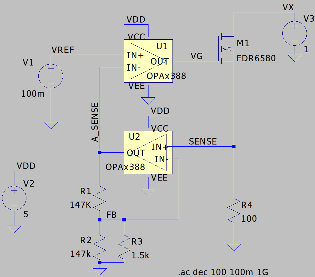
I am trying to analyze an active load circuit designed for the lowest current possible. Schematic in the picture.
I tried to amplify the sensed voltage (by 100 / 40dB) to increase the sensitivity. Yes, I know this circuit can easily oscillate...

My question is, which node should I split to break the loop for loop gain / AC analysis? Is it SENSE, A_SENSE or VG ?
I mean, standard AC simulation with DC source DC=0 AC=1 in the loop.

Thanks
Shlooky
pic.png
 

Not to spoil your fun, but a few things. Op amp will probably be unstable from the get-go, direct-driving that fat FET gate. And a weakly driven FET will make a load which doesn't handle dynamics well.
 

Not to spoil your fun, but a few things. Op amp will probably be unstable from the get-go, direct-driving that fat FET gate. And a weakly driven FET will make a load which doesn't handle dynamics well.
Dick the input C to MOSFET is only 4000 pF, I dont see any problem here 🔥
And spec sheet shows only 80% overshoot at 1000 pF, lots of signal fidelity,
tons of margin.....

But to OPs credit he knows thats an issue. I just could not resist being a wiseass :).


Regards, Dana.
 
Last edited:

Agree with dick_freebird about possible stability issues. Often some loop compensation for U1 is necessary. But loop gain analysis will show.

Is zero load impedance in drain circuit a realistic assumption for the final application? Particularly inductive load can affect loop gain.
 

Hi guys,

Thanks for your inputs.

The circuit is designed to regulate very small currents / voltages. Range of mA / units of V.
My MOSFET is actually ALD210808 - P_diss up to 0.5W. Its input C is mere 15 pF. I could not find a model online, so I just used the smallest MOSFET in original LTSpice database.

The drain will be connected directly to VX, as the the MOSFET itself is a controlled load. Will update on loop gain / stability analysis very soon.

Thanks again

Shlooky
 

I'm not sure if you already fully understand what you're doing. The ALD210808 is a very expensive precision device. However, in your circuit, all precision is created by the sensing resistor and the sense amplifier. The ALD's excellent matching and DC specs - except maybe for leakage current - are completely irrelevant for your application. Besides that, the array will complicate the pcb layout and the high Rdson may limit the maximum current through the load. Don't worry (yet) about the mosfet capacitance. You can probably easily get it right up to several tens of kHz. If possible, switch to almost any other very cheap small mosfet.

Since you're already aware of possible stability issues, I'ld suggest you gain a better understanding of the loop gain, poles and zeros before starting the simulation. There are many places in the circuit where a capacitor or resistor could be added and the simulation does not tell you directly which is the best.

Also, don't forget the impact of load impedance on the mosfet Cgd. You might wish to use a mosfet that comes with a decent spice model.
 
Last edited:

I'm not sure if you already fully understand what you're doing. The ALD210808 is a very expensive precision device. However, in your circuit, all precision is created by the sensing resistor and the sense amplifier. The ALD's excellent matching and DC specs - except maybe for leakage current - are completely irrelevant for your application. Besides that, the array will complicate the pcb layout and the high Rdson may limit the maximum current through the load. Don't worry (yet) about the mosfet capacitance. You can probably easily get it right up to several tens of kHz. If possible, switch to almost any other very cheap small mosfet.

Since you're already aware of possible stability issues, I'ld suggest you gain a better understanding of the loop gain, poles and zeros before starting the simulation. There are many places in the circuit where a capacitor or resistor could be added and the simulation does not tell you directly which is the best.

Also, don't forget the impact of load impedance on the mosfet Cgd. You might wish to use a mosfet that comes with a decent spice model.

Hi there,

I am trying to design a programmable DC load that can regulate small currents / small power dissipation (as low as possible). It will be used in low-voltage / low-power projects. I know that literally any MOSFET would work here. I picked ALD MOSFET because in its datasheet, it has clearly defined transfer characteristics in sub-threshold region, low C_GS and Miller C_GD and low threshold voltage. The price is not really an issue. We won't go to mass production with this....
We are trying to find the lowest current value that can be regulated with this simple topology.

The sensing resistor is high precision, low temperature coefficient.
OPAMPs are rail-to-rail, low offset, low noise, etc. Probably an overkill, too.

I found out that the SPICE model of the opamp is probably garbage (picture attached). With identical conditions as in the datasheet (symmetrical +/-2.5V = 5V, inputs in the middle, load = 10k + 100pF, AC goes to inverting input according the phase diagram), the model gives drastically different results for open loop gain. If I am not making any fundamental mistake here, I believe I can flush the whole simulations down the toilet....

Screenshot 2023-03-06 16:40:52.png


We built the circuit on breadboard and the regulating opamp (U1 in the original post) needs to be connected as an integrator. So far it seems to work properly...

Will update later....
 

Open loop gain analyses are critically dependent on a good
operating point. Even a little bit of systematic Vio can ruin a
testbench like you show.

I prefer a scheme where you place a large (LARGE) inductor
in the (OUT)-(IN-) path to close the loop at DC, and forget
about 1Hz artifacts since nothing ever matters there except
1/f noise. Now you'll "auto-center" the OP analysis and get a
robust gain/phase redult (for circuits that are essentially the
same, i.e. loop closes to ~ Vio).

Take your Vin(diff) with a vcvs off the terminals and now it's
all Calculator (or math-on-vectors or math-in-plot-arg) to get
classical Bode plots.

Thank you, man!
I simulated the open loop gain with schematic very similar to what you described above... and the results look VERY close to the datasheet.

Lesson learned...

Thanks again

Screenshot 2023-03-06 21:18:02.png
 

Status
Not open for further replies.

Part and Inventory Search

Welcome to EDABoard.com

Sponsor

Back
Top