Continue to Site

Welcome to EDAboard.com

Welcome to our site! EDAboard.com is an international Electronics Discussion Forum focused on EDA software, circuits, schematics, books, theory, papers, asic, pld, 8051, DSP, Network, RF, Analog Design, PCB, Service Manuals... and a whole lot more! To participate you need to register. Registration is free. Click here to register now.

[SOLVED] Looking for DXF to Gerber Conversion

Status
Not open for further replies.

mkannu

Newbie level 3
Joined
Sep 1, 2016
Messages
3
Helped
0
Reputation
0
Reaction score
0
Trophy points
1
Activity points
25
Dear All,

I am a new to electronics. Trying to do a hobby project. I have a very simple design in dxf. But to make production everyone is asking for a Gerber file. Anyone please help me or guide me with this. I attached the dxf files and PDF preview.

thanks
Mujib Housing Ver4 Dimensions.jpgView attachment Housing Ver4 Dimensions.pdfView attachment Housing Ver4.rar
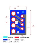
 

Before you can Gerber it, those large pads - are they plated through? If so the annular ring looks too small.

Also before telling you how to produce Gerbers we need to know what software was the board drawn in?
 

The representation image is not up to scale.To give you understanding i just made that with my hand.
The original file is scaled version and that is created in AutoCAD.
Can you tell me how I can convert the AutoCAD DXF to Gerber. Is it easy?
 

The appended dxf is useless because it has all data in a single layer.

PCB layout data must have separate layers for

each copper layer (apparently 1 in your design)
soldermask(s)
silkscreen ("marking")
board outline
drills

Drill data must be probably manually converted because a file with x/y coordinates and tool number is expected. (Excellon file)

The other data should be sketched as closed and filled polygons, then you have a chance to convert it with a gerber tool or import function of a cad tool.

Your layout is so simple that it's possible easier to redraw it in a free cad tool.
 

they are not plated through. Just holes to solder wires. It is a single layer PCB. I have created scaled version In AutoCAD.
 

Your using the wrong tool.

Download Eagle, Kicad, Designspark or any of the other free PCB programs and redo it as a PCB and not a mechanical drawing.

Or use Google and search on how to make Gerbers from AutoCAD,
 

Status
Not open for further replies.

Part and Inventory Search

Welcome to EDABoard.com

Sponsor

Back
Top