Continue to Site

Welcome to EDAboard.com

Welcome to our site! EDAboard.com is an international Electronics Discussion Forum focused on EDA software, circuits, schematics, books, theory, papers, asic, pld, 8051, DSP, Network, RF, Analog Design, PCB, Service Manuals... and a whole lot more! To participate you need to register. Registration is free. Click here to register now.

[SOLVED] Logical effort meaning

Status
Not open for further replies.

iVenky

Advanced Member level 2
Joined
Jul 11, 2011
Messages
584
Helped
37
Reputation
76
Reaction score
35
Trophy points
1,318
Location
College Station, Texas
Activity points
6,124
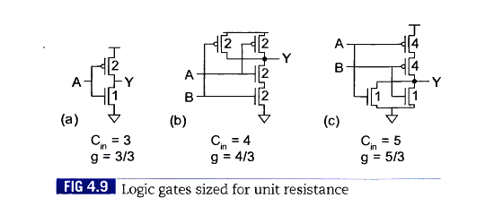
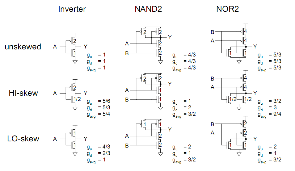
Recently I read about logical effort but I quite couldn't understand that.
Ivan Sutherland says
"The logical effort of an inverter is taken to be one.The logical effort for any other logic function describes how much worse it is than an inverter at producing output current,given an equivalent amount of input capacitance".

Why does the effort of producing the same current varies with the logic function?
Also please explain me this definition.

Thanks in advance.
 
Last edited:

You can treat the LE as the ratio of output resistance to input capacitance.
For an inverter, you can halve the output resistance by doubling the size of the transistors, but that will also double the input capacitance, hence always giving an LE of one.
Giving an example of a NAND gate, for same output resistance as compared to that of an inverter, the PMOS should have the same size, but the NMOS has to be double as there are 2 NMOS in series. So the input sees 2 PMOS and 2 NMOS (with double the size), giving a much larger input capacitance as that of an inverter with same output resistance.
 

I read that the logical effort of NAND (with two inputs ) is 4/3 and for NOR it is 5/3. How can you say that?

Thanks in advance.
 

I am a bit rusty with my definitions. Apologies on that.
Google states that logical effort is a ratio of capacitance relative to that of an inverter with the same driving capability.
Assuming Kp/Kn is 2, then an inverter will see 3 units of input capacitance (one from NMOS and 2 from PMOS)
Each input of the NAND will see a similar sized PMOS, but a double-sized NMOs, ie total 4 units.
That's where you get the 4/3 from.
 

I still don't get how you got 4 units.
In inverter if you add all W/L ratio you will get 3. I understand that.
But in a similar fashion if you do it for NAND gate (where you have W/L ratios of 2,2 for NMOS and 2,2 for PMOS) you get 8 units.

Could you please clear my doubt?

Thanks in advance.
 

I still don't get how you got 4 units.
In inverter if you add all W/L ratio you will get 3. I understand that.
But in a similar fashion if you do it for NAND gate (where you have W/L ratios of 2,2 for NMOS and 2,2 for PMOS) you get 8 units.

Could you please clear my doubt?

Thanks in advance.
8 units for 2 inputs, ie 4 units per input.
 
  • Like
Reactions: iVenky

    iVenky

    Points: 2
    Helpful Answer Positive Rating
I read that the logical effort of NAND (with two inputs ) is 4/3 and for NOR it is 5/3. How can you say that?

From: Weste / Harris: "CMOS VLSI DESIGN", 3rd edition, pp. 166-167:

Figure 4.9 shows inverter, NAND, and NOR gates with transistor widths chosen to achieve unit resistance, assuming pMOS transistors have twice the resistance of nMOS transistors. The inverter presents 3 units of input capacitance. The NAND presents 4 units of capacitance on each input, so the logical effort is 4/3. Similarly, the NOR presents 5 units of capacitance, so the logical effort is 5/3.
 

Awesome man. Now as I asked in the beginning of this thread what do you mean by this sentence?
"The logical effort for any other logic function describes how much worse it is than an inverter at producing output current,given an equivalent amount of input capacitance"


Why does the output current varies with the logic function? I just couldn't understand it's relationship with input capacitance.

Thanks in advance
 

"The logical effort for any other logic function describes how much worse it is than an inverter at producing output current,given an equivalent amount of input capacitance"

Why does the output current varies with the logic function? I just couldn't understand it's relationship with input capacitance.

Within this LE consideration, the output current (capability) does not vary, the output current (or impedance) -- for any gate which is to be compared to an inverter -- is kept constant and equal to the inverter's output current. As checkmate explained above, for this goal you need respectively more and/or larger transistors. The input capacitance of all the transistors needed to achieve the standardized output current in relation to an inverter's input capacitance (3 std. cap. units) is the LE of the resp. gate input.

This is standardized for Kn/Kp=2, i.e you need 2 PMOS units to deliver the same current as 1 NMOS unit, which also means 2 std. PMOS input cap units in comparison to 1 std. NMOS input cap. unit -- that's why an inverter needs 3 input cap. units. The LE is always related to 1 single input.

For different output drive capabilities the LE comparison values may be different, see this image below:


Also for complex gates, different inputs could own different LE values.
HTH! erikl
 
  • Like
Reactions: iVenky

    iVenky

    Points: 2
    Helpful Answer Positive Rating
Within this LE consideration, the output current (capability) does not vary, the output current (or impedance) -- for any gate which is to be compared to an inverter -- is kept constant and equal to the inverter's output current. As checkmate explained above, for this goal you need respectively more and/or larger transistors. The input capacitance of all the transistors needed to achieve the standardized output current in relation to an inverter's input capacitance (3 std. cap. units) is the LE of the resp. gate input.

This is standardized for Kn/Kp=2, i.e you need 2 PMOS units to deliver the same current as 1 NMOS unit, which also means 2 std. PMOS input cap units in comparison to 1 std. NMOS input cap. unit -- that's why an inverter needs 3 input cap. units. The LE is always related to 1 single input.

For different output drive capabilities the LE comparison values may be different, see this image below:


Also for complex gates, different inputs could own different LE values.
HTH! erikl


Hi,
I understood the logical efforts in the unskewed procedure. But I don't understand the same in the Hiskew and Low-Skew.
Please explain
 

I understood the logical efforts in the unskewed procedure. But I don't understand the same in the Hiskew and Low-Skew.
Please explain

You're right: nor do I. And I don't remember where I got this table from.
Perhaps may help you; I didn't retrace the equations.
 

Status
Not open for further replies.

Part and Inventory Search

Welcome to EDABoard.com

Sponsor

Back
Top