Alon123
Newbie
Hi Everyone,
I am struggling with this question in which I need to understand what is the route with the least effort (H).
Usually, I'm given a route but it's very simple to calculate, because all the other inputs of the logical gates are regular inputs without any logical gates connected to them, like in this example:

The main difference and what I am struggling with, is in the example above the route is clear, and the legs of the logical gates are just regular inputs..
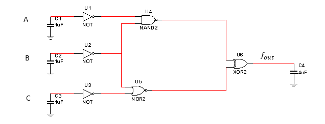
The circuit which I need to analyze is this:

And the question is which route has the least effort (H) - A,C, or they both the same.
My hunch is that they're both the same, but I can't figure out how to calculate it.
I think the fan-out (f) is the same for both routes - 4/1=4 (I might be wrong here so please let me know if I do).
But I'm not sure how to calculate the logical effort (G) in the routes.
For example, if I look at route A, so the first logic gate is a NOT (g=1), and the next one is NAND2 (g=4/3), but, the other input of the NAND also has a NOT gate connected to it. In my opinion, this shouldn't matter (because again, g of NOT is 1). But when I look further to this route I have a XOR2 (g=4). so far, G=g1*g2*g3=1*4/3*4=16/3, and H=G*F=64/3.
But I don't think it's right, since the other input of the XOR2 is connected to route C, so it has a NOR and a NOT beforehand.
So finally - my question is how do you calculate the effort of a route, if it has more logical gates from the other input?
Thanks in advance!!
I am struggling with this question in which I need to understand what is the route with the least effort (H).
Usually, I'm given a route but it's very simple to calculate, because all the other inputs of the logical gates are regular inputs without any logical gates connected to them, like in this example:
The main difference and what I am struggling with, is in the example above the route is clear, and the legs of the logical gates are just regular inputs..
The circuit which I need to analyze is this:
And the question is which route has the least effort (H) - A,C, or they both the same.
My hunch is that they're both the same, but I can't figure out how to calculate it.
I think the fan-out (f) is the same for both routes - 4/1=4 (I might be wrong here so please let me know if I do).
But I'm not sure how to calculate the logical effort (G) in the routes.
For example, if I look at route A, so the first logic gate is a NOT (g=1), and the next one is NAND2 (g=4/3), but, the other input of the NAND also has a NOT gate connected to it. In my opinion, this shouldn't matter (because again, g of NOT is 1). But when I look further to this route I have a XOR2 (g=4). so far, G=g1*g2*g3=1*4/3*4=16/3, and H=G*F=64/3.
But I don't think it's right, since the other input of the XOR2 is connected to route C, so it has a NOR and a NOT beforehand.
So finally - my question is how do you calculate the effort of a route, if it has more logical gates from the other input?
Thanks in advance!!