Continue to Site

Welcome to EDAboard.com

Welcome to our site! EDAboard.com is an international Electronics Discussion Forum focused on EDA software, circuits, schematics, books, theory, papers, asic, pld, 8051, DSP, Network, RF, Analog Design, PCB, Service Manuals... and a whole lot more! To participate you need to register. Registration is free. Click here to register now.

Load switch based on N-MOS or P-MOS as Pass Transistor

Status
Not open for further replies.

malli_1729

Full Member level 5
Joined
Feb 13, 2007
Messages
252
Helped
48
Reputation
96
Reaction score
46
Trophy points
1,308
Location
INDIA
Activity points
3,292
Hi,

For one of my project, i am looking at Switching power to the extender boards from main board.
I am doing the feasibility analysis of Load Switch or discrete implementation using nMOS or pMOS.In that process i have encountered this point which i am not clear.

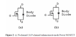
"When using an N−channel MOSFET in a load switch circuit, the drain is connected directly to the input voltage rail and the source is connected to the load" and
"When using a P−channel MOSFET in a load switch circuit (as in Figure 1, the source is directly connected to the input voltage rail and the drain is connected to the load"

My doubt is:
When we are using nMOS anyway we need extra rail to be connected to Gate terminal so, that Vgs >= Vth +vin(Load to be switched). So, this doesn't matter whether we connect input(vin) to either S or D ( we can intercahnge S and D). any other consideration why D will be connected to Vin and S will be Load ?
Same for P-MOS also.
 

The only possibility that I can think of is that in discrete transistors body may always be connected to source. There is a diode from the body( p-type) to the drain(n t-type). Since body is connected to the source, there is a diode from the source (p connection) to the drain (n connection). If input is connected to the source, it will not be able to drive the load, because of this diode getting forward biased.
 

Hi,

Thanks for the reply.

So, always for n-MOS current has to flow Drain to Source ( then only it will flow in the channel), for P-MOS current has to flow from Source to Drain .
As a matter of enthusiasm, Is there any other reason for this.
 

Attachments

  • BodyDiode.png
    BodyDiode.png
    33.7 KB · Views: 70

In NMOS channel is of n-type, so the charge carriers electrons flow from lower potential terminal (which is called source) and collected by higher potential terminal (called drain), so the conventional current direction is from drain to source.
In PMOS, channel is of p-type and holes move from higher potential terminal (called source) to lower potential terminal (called drain). So the conventional current direction is also source to drain.
 

I don't have much understanding of the MOSFET's. So, my questions are little weird. bare with me.
Generally,

Potential you have referred, is applied by us ( in the actual circuit, which can be applied in anyway i. S can be Positive than D or vice versa),
or you mean MOSFET will have any internal potentials.
 

An N-channel MOSFET can be used as a switch to control current from DRAIN to SOURCE. Current will flow from DRAIN to SOURCE when the potential at DRAIN is higher than the potential at SOURCE.

You apply the potential difference.
 

Integrated plain FETs are symmetric usually and can be
polarity-swapped (S,D) without care. Power MOSFETs
are asymmetric in voltage blocking -and- have the body
hard-connected to source. You need to determine what
you're talking about using, and understand their real
attributes (not theories based on simplified / assumed
device characteristics).

A NMOS, positive load switch will need a boosted rail
for the gate drive.

There are products out there for these applications,
both integrated and "everything-but-the-big-FET".
 

Status
Not open for further replies.

Part and Inventory Search

Welcome to EDABoard.com

Sponsor

Back
Top