Welcome to our site! EDAboard.com is an international Electronics Discussion Forum focused on EDA software, circuits, schematics, books, theory, papers, asic, pld, 8051, DSP, Network, RF, Analog Design, PCB, Service Manuals... and a whole lot more! To participate you need to register. Registration is free. Click here to register now.
Hi, wonder if anybody come across any plot for LNA IIP3 (sim or measured)? If yes, how does it look like? Have an example, but do not know if it's correct?
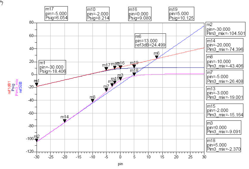
The graph that you get is correct. The deep in the characteristic is due to the phases of the third and fifth IMD products. You can minimize this deep placing the bias of the amplifier closer to Class A operating point.
This phenomenom is called "Sweet Spot" where the transistor is in the region between weak inversion and saturation, so the third and fifth derivatives of gm is going to 0 so the IIP3 is improved.
This site uses cookies to help personalise content, tailor your experience and to keep you logged in if you register.
By continuing to use this site, you are consenting to our use of cookies.