Continue to Site

Welcome to EDAboard.com

Welcome to our site! EDAboard.com is an international Electronics Discussion Forum focused on EDA software, circuits, schematics, books, theory, papers, asic, pld, 8051, DSP, Network, RF, Analog Design, PCB, Service Manuals... and a whole lot more! To participate you need to register. Registration is free. Click here to register now.

Little help with circuit analysis of amplifier

Status
Not open for further replies.

gonsays

Newbie level 5
Joined
Mar 25, 2015
Messages
10
Helped
0
Reputation
0
Reaction score
0
Trophy points
1
Activity points
83
Hello guys,

I'm new here and I'm on an introductory course to Analogic Integrated Systems.

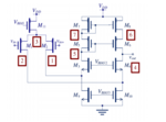
I have the following circuit of a Two-stage CMOS OTA folded cascode amplifier:

circuit2.png

The table regarding the specifications of this circuit are the following:

specifications-table.PNG


------------------------------------------------------------------------------------------

As you can see on the circuit, there are two currents in black (I1 and I2). From the specifications table we know that Idd=400uA. This way we will have Idd=I1+I2.

I woul really appreaciate your help regarding the analysis or values of the dimensions for the transistors in order for this to happen.

Any help is really appreciated, because with so many specifications I don't know how to start the circuit analysis :bang:

Thank you very much in advance guys!!

Regards,
Gz
 

Attachments

  • circuit.PNG
    circuit.PNG
    27.9 KB · Views: 119

Hi there

the current I1 will be determined by the biasing circuit, in this case a current mirror, (not shown) that gives a voltage to VBIAS node

On the other hand, the biasing circuit that sets VBIAS2 determines I1+I2.
This means that 400uA will be the value of your ground current, and half of it will flow through M9 and M10 respectively.

The amount of current you give in your differential pair will play a role in the gain and BW of your amplifier.

I hope this helps
 
Hello,

Thank you very much for the help :)

I would need to have a slew-rate of 200 V/us and I think I should start by the slew-rate to determine the needed current for I1 and I2, how can I calculate it on this circuit?

Any help is appreciated :)
 

Hi

Slew rate depends on the output capacitance that you need to drive. It is calculated as SR= I/Cout.
What do you need to drive with this circuit?
 

Hello guys,

I woul really appreaciate your help regarding the analysis or values of the dimensions for the transistors in order for this to happen.

Any help is really appreciated, because with so many specifications I don't know how to start the circuit analysis :bang:

Hi gonsays,

If you want to find out the transistor dimensions, you would have to use the MOS Current equation.
For that you would need the process parameters like Kn, Kp, Cox etc.
For that you would have to run some basic simulations instead of trying to build an Op-Amp first.

Try out some basic simulations and other circuits before trying out more complex stuff.

The Opamp would require a bias circuit to provide the bias voltages(you could still use voltage sources but they wont work across corners.)

There are other posts on edaboard that will help you out with these things.
 

Status
Not open for further replies.

Similar threads

Part and Inventory Search

Welcome to EDABoard.com

Sponsor

Back
Top