Continue to Site

Welcome to EDAboard.com

Welcome to our site! EDAboard.com is an international Electronics Discussion Forum focused on EDA software, circuits, schematics, books, theory, papers, asic, pld, 8051, DSP, Network, RF, Analog Design, PCB, Service Manuals... and a whole lot more! To participate you need to register. Registration is free. Click here to register now.

Linearization techniques in Razavi <Design of Analog CMOS Integrated Circuits> Ch13

Status
Not open for further replies.

fightshan

Junior Member level 3
Joined
Jul 30, 2013
Messages
28
Helped
0
Reputation
0
Reaction score
0
Trophy points
1
Location
China
Activity points
260
Linearization techniques in Razavi <Design of Analog CMOS Integrated Circuits> Ch13

I am studying a high speed Track&Hold circuits in a high speed F/I ADC. In the T&H circuit , there are two buffers ,the input_buffer to isloate kickback noise and the output_buffer to supply an appropriate driving ability for the ADC core.
I select a NMOS source follower as the input_buffer, and a unit_gain op_amp which works in open loop state as the output_buffer.
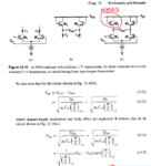
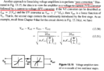
The problem I meet now is the bad linearity of output buffer. In the Chapter13 of <Design of Analog CMOS Integrated Circuits> written by Razavi, a linearization technique called "post_correction" is introduced by Razavi, I am interested in this structure, but there is just a small section of this in the chapter ,and Razavi didn`t mention any reference. So, I wonder anyone can give more information about this "post_correction" tech?
I really appreciate anyone can discuss this with me!
1.png
2.png
3.png
 

Re: Linearization techniques in Razavi <Design of Analog CMOS Integrated Circuits> Ch

... a unit_gain op_amp which works in open loop state as the output_buffer.
Is it a unity_gain op_amp? Such op_amps usually are closed loop op_amps with full feedBack, or perhaps it is a near-unity_gain op_amp, perhaps a source-follower like your input buffer? If it's the latter, why not use the linearization circuit like Figure 13.16 (c)?

Other possibility is a real buffer op_amp, i.e. an OTA with a class AB output stage (to achieve good output drive) and full feedBack, which gives you high linearity and also high bandwidth because of the unity_gain.
 

Re: Linearization techniques in Razavi <Design of Analog CMOS Integrated Circuits> Ch

Is it a unity_gain op_amp? Such op_amps usually are closed loop op_amps with full feedBack, or perhaps it is a near-unity_gain op_amp, perhaps a source-follower like your input buffer? If it's the latter, why not use the linearization circuit like Figure 13.16 (c)?

Other possibility is a real buffer op_amp, i.e. an OTA with a class AB output stage (to achieve good output drive) and full feedBack, which gives you high linearity and also high bandwidth because of the unity_gain.

4.jpg

Thank you for your reply!

It is a near unit gain op-amp,because I select a NMOS source follower as the inputbuffer, whose gain is slightly less than 1, and to maintain the unit gain of the entire TH circuit , I have to select a opamp which does not have a accurate unit-gain.

Your seggestion that I can select another source-follower as the output buffer is nice, and I did consider a PMOS source follower as the output buffer, however, as the Figure.4 I upload shows, I need to maintain the output common voltgage equal to the input common voltage ,which is 1.25V. So, NMOS follower has a drop of Vcm, and PMOS follower has rise of Vcm, and I don`t know how to make the drop and rise equal, and considering mismatch and different corners of the CMOS process, I don`t think that the output common voltage of TH circuit can be maintained at precise 1.25V after tape out.

Considering above , I select an op-amp as the outputbuffer.

I agree with your argument that high linearity need a full feedback , but in my application, the sampling frequency is 1GHz, closed loop op-amp has an enough bandwidth for this speed?

So, I still consider the linearization circuit like Firgure 13.16.
 

Re: Linearization techniques in Razavi <Design of Analog CMOS Integrated Circuits> Ch

I assume you have an anti-aliasing filter before the mux you have shown in the image. Linearity will be a concern since you are using source follower in open loop configuration. So you need to precisely cancel the non linearity introduced by the input buffer at the output buffer. But if you are using two different kind of buffers, how do they track and cancel each other's effect?

Setting common mode voltages should not be an issue as you can do so by CMFB loops at the input and output buffers.

As far as the linearity of the output buffer is concerned, it is more important to make it an inverse of the input buffer's behavior to hit high linearity numbers since the linearity of a source follower is very poor, which you might already be seeing by now. If the linearity is of so much concern (say 80-90 dBc), I would go for a ADC buffer->TH->ADC core, where the buffer is an opamp in feedback which is enough to drive the TH impedance. Having multiple stages also worsens the SNR and hence SINAD of the ADC.

Thank you for your reply.

My work is based on 0.18um triple well CMOS process, and I hope the sample frequence can be up to 1GS/s. As I know , traditional closed loop track/hold circuit based on 0.18um process is difficult to meet this speed (it`s easy to find some references using the closed loop topology used in TH circuits, but the sample speed is uaually multi hundred MHz.)

I don`t know how to add the CMFB circuit to source follower, and I never saw this circuit before. Can you give me some reference about this?

You said the linearity of source follower is very poor, I agree this at first , because Razavi said " typical source followers suffer from several percent of nonlinearity" , however, the NMOS source follower which is used here is slightly different from the typical one, the simulated ENOB of source follower can be up 12bit, so I don`t worry about this.

Multiple stages do worsen the SNR and SINAD(or SNDR), but , due to the input buffer NMOS source follower has a drop of Vcm, I have to select another output buffer to compensate it.

Actually, your idea "ADC buffer->TH->ADC core" is nice, but this solution is suitable for closed loop TH, then again, the bandwidth of closed loop can meet the 1GS/s requirement?
 

Re: Linearization techniques in Razavi <Design of Analog CMOS Integrated Circuits> Ch

... Considering above , I select an op-amp as the outputbuffer.

I agree with your argument that high linearity need a full feedback , but in my application, the sampling frequency is 1GHz, closed loop op-amp has an enough bandwidth for this speed?
Yes, if the rest of your circuit can cope with this bandwidth.

So, I still consider the linearization circuit like Firgure 13.16.
Why not, but will it provide enough drive strength as output buffer?
 

Re: Linearization techniques in Razavi <Design of Analog CMOS Integrated Circuits> Ch

Yes, if the rest of your circuit can cope with this bandwidth.


Why not, but will it provide enough drive strength as output buffer?

I don`t know, that is the reason why I come here to discuss the topic and hope to get some useful information or some reference.

By the way, besides bandwidth, I also take the input impendence and out impendence into consideration. In my opinion, the buffer should have a large input impendence and a small output impendence, and given the large signal response,the buffer should have enough current (to achieve enough slew rate). The above is my consideration about buffer, is it right? Or, I miss any other aspect?
 

Re: Linearization techniques in Razavi <Design of Analog CMOS Integrated Circuits> Ch

Yes, you are right. The input buffer should have enough slew rate to drive the switch cap load.

For setting the common mode voltages, hope this helps. https://obrazki.elektroda.pl/5167871000_1448865862.jpg
 
Re: Linearization techniques in Razavi <Design of Analog CMOS Integrated Circuits> Ch

Yes, you are right. The input buffer should have enough slew rate to drive the switch cap load.

For setting the common mode voltages, hope this helps. https://obrazki.elektroda.pl/5167871000_1448865862.jpg

Thank you, the picture you give is helpful.

Besides enough slew rate, how to consider the output impendence of inputbuffer? What is the exact meaning of "drive capability"?
 

Re: Linearization techniques in Razavi &lt;Design of Analog CMOS Integrated Circuits&gt; Ch

By the way, besides bandwidth, I also take the input impendence and out impendence into consideration. In my opinion, the buffer should have a large input impendence and a small output impendence, and given the large signal response,the buffer should have enough current (to achieve enough slew rate). The above is my consideration about buffer, is it right? Or, I miss any other aspect?

Yes, I think you're totally right!

- - - Updated - - -

For setting the common mode voltages, hope this helps. https://obrazki.elektroda.pl/5167871000_1448865862.jpg

Do you think it's correct to connect two outputs?
 

Re: Linearization techniques in Razavi <Design of Analog CMOS Integrated Circuits> Ch

Yes, I think you're totally right!

- - - Updated - - -


Do you think it's correct to connect two outputs?

From my point of view , I take the PMOS source follower as a dummy follower whose function is to sustain the common voltage but not a output buffer.

What`s your opinion?

Actually, I hope the explaination of ASM012 , after all, that is his (or her?) idea.
 

Re: Linearization techniques in Razavi <Design of Analog CMOS Integrated Circuits> Ch

In the figure that I have uploaded, the output of the opamp is used to set the output common mode of the previous stage to whatever the value that is required for it to set the output common mode of the pmos buffer to required value (1.25V in this case). Vocm is an input for the previous stage (input to the CMFB of the previous stage). I think it should work. Please let me know if I am wrong. https://obrazki.elektroda.pl/2424772500_1448900298.jpg
 

Re: Linearization techniques in Razavi <Design of Analog CMOS Integrated Circuits> Ch

Vocm is an input for the previous stage (input to the CMFB of the previous stage). I think it should work. Please let me know if I am wrong. https://obrazki.elektroda.pl/2424772500_1448900298.jpg

Sure, this should work. I didn't recognize that Vocm is an input, sorry.

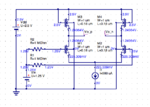
But isn't it a bit too complex? I guess that fightshan's image #2 Figure 13.16 (c) should also work:
Figure_13.16c_example.png
Just an example!
 

Status
Not open for further replies.

Part and Inventory Search

Welcome to EDABoard.com

Sponsor

Back
Top