Continue to Site

Welcome to EDAboard.com

Welcome to our site! EDAboard.com is an international Electronics Discussion Forum focused on EDA software, circuits, schematics, books, theory, papers, asic, pld, 8051, DSP, Network, RF, Analog Design, PCB, Service Manuals... and a whole lot more! To participate you need to register. Registration is free. Click here to register now.

Leakage current from ESD protection

Status
Not open for further replies.

anger5

Newbie level 4
Joined
Feb 20, 2010
Messages
5
Helped
0
Reputation
0
Reaction score
0
Trophy points
1,281
Activity points
1,321
I want ask if there is some leakage current from ESD protection?
I have a circuit, which is designed to use capacitor to hold the sampling voltage. But after sampling, the voltage drops quickly. Which means some current must go some path to ground to discharge the capacitor. I have already check my circuit, the only reason thing I found may be the ESD protection circuit would have some leakage current in my IC design.

However, I am not sure. Have anyone can help me to find the answer? Thanks.
 

"Some", always. Question is "how much?". Intact ESD diodes
ought to draw sub-nA (temperature dependent) but one that
has already been abused, or a test escape, could pull more.

You should calculate the leakage magnitude as Csample*dV/dt
and see what kind of leakage it indicates. A circuit that depends
on sub-pA leakages had better be designed and treated right.
But you also can't discount leakages on that order, from your
sample switches - I've been seeing tens of nA leakages on short
channel FETs in the 180nm nodes. Models rarely do a good
job of leakage currents aside from the subthreshold slope part
of it.

If you really suspect the ESD clamps, take a unit and have
your FA lab cut away the clamps (if you haven't slabbed top
metal over it all, and can get to them). Run some pin I-Vs
and see how these compare to your calculated Ileak above.
 

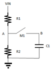
a.png
This is a circuit I used. External C1 is 10nF~100nF. External R1 and R2 are 10Meg ohm. Switch is integrated in the chip. A and B node are connected ESD protection circuit, which are PADs we can access.
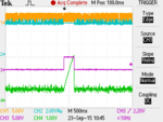
F0082TEK.png
The purple one is VIN, and green one is a sampling voltage.
Is this possibly caused by switch M1? if non-zero voltage cross the switch when ON state.
 
Last edited by a moderator:

The test circuit is somehow incomplete. How do you measure the capacitor voltage?
 
  • Like
Reactions: anger5

    anger5

    Points: 2
    Helpful Answer Positive Rating
Good point; 1 10Mohm scope probe could ruin your day,
dwarfing any ESD element's contribution.

Any chance you can show the -real- schematic? With
your MOSFET switch, things like body potential may
matter. But to me, if VIN is your analog voltage then
the switch looks to be always-closed, and the "sample"
is just following that step waveform as best it's able.
Or, if VIN is the S/Hb control, then what is the test
analog waveform to challenge the sampling and holding?
 

The test circuit is somehow incomplete. How do you measure the capacitor voltage?

I just used the differential probe across B node to ground.
 

I measured again today. I am sure it is caused by probe. When I took away the probe, everything works well. Thanks.
 

Status
Not open for further replies.

Similar threads

Part and Inventory Search

Welcome to EDABoard.com

Sponsor

Back
Top