artiste
Newbie level 6
Hi,
I've to design a kit of test-structures for modeling CPW lines on high-resistivty silicon wafer. The goal is to perform de-embedding with TRL, Half-Thru method, etc...
I have some basic questions about the layout of the de-embedding structures.
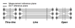
For the OPEN structure:
- What is the distance that must be considered typical for interruption? 10μm, 20 microns, 100 microns?
- Is this distance related to the width and gap of the coplanar line?
- How this affects the distance de-embedding?
How wide you recommend for the ground of the coplanar lines? 1 time the ground-to-ground distance of the coplanar to limit the surface structures of test? Or increase to 2x the distance for accuracy?
Thank you for your answers
I've to design a kit of test-structures for modeling CPW lines on high-resistivty silicon wafer. The goal is to perform de-embedding with TRL, Half-Thru method, etc...
I have some basic questions about the layout of the de-embedding structures.
For the OPEN structure:
- What is the distance that must be considered typical for interruption? 10μm, 20 microns, 100 microns?
- Is this distance related to the width and gap of the coplanar line?
- How this affects the distance de-embedding?
How wide you recommend for the ground of the coplanar lines? 1 time the ground-to-ground distance of the coplanar to limit the surface structures of test? Or increase to 2x the distance for accuracy?
Thank you for your answers