xun36
Newbie level 2
w/l transistor
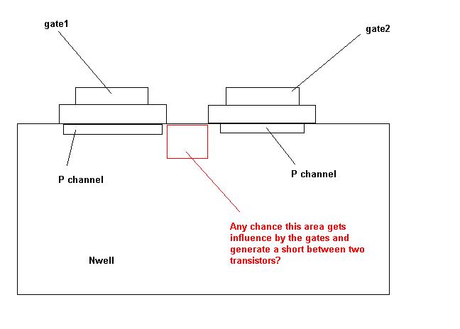
Hi,
I have two or more transistors with W=0.5 L=50. I want to put them in the layout one by one aligned by their length. But in this case the the channels of two MOS gets very close. Is there any risk? Like the gate will reverse the Nwell to Ptype and make a short inbetween the two N channel?
Thanks.
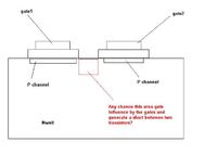