Alfie_Guo
Newbie
Hi there,
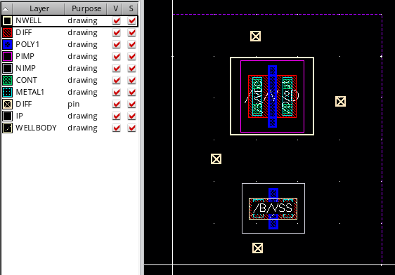
I am learning how to make integrated circuit design in Cadence, and starting with an inverter. For the layout design, I noticed that someone aligns the pins(Vin, Vout, Vdd, Vss, etc.) to the metal layer while someone aligns them to the poly layer. Which one is correct? What is the difference between selecting different layers for the pins?
For my design, I imported the components directly from the schematic design. Yet, I don't know exactly which layer are these pins assigned to.
Thank your for asistant.
Best regars,
Aofei