Continue to Site

Welcome to EDAboard.com

Welcome to our site! EDAboard.com is an international Electronics Discussion Forum focused on EDA software, circuits, schematics, books, theory, papers, asic, pld, 8051, DSP, Network, RF, Analog Design, PCB, Service Manuals... and a whole lot more! To participate you need to register. Registration is free. Click here to register now.

Layer 6 Capacitance in Cadence in 180nm

Status
Not open for further replies.

KingDarius6288

Junior Member level 2
Joined
May 10, 2019
Messages
24
Helped
0
Reputation
0
Reaction score
0
Trophy points
1
Activity points
210
Hi,

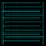
Attached is an interdigitated electrode, implemented using metal 6 layer in 180nm tech, with a capacitance value of 6fF. It should generate a 70% change in the gain of an OTA, but when I connect it to the OTA, nothing happens. It seems that the Cadence does not recognize it as a capacitance. Am I missing some layer in the electrode layout?
In other words, for the cadence to consider the capacitance of the electrode, should I add a specific layer or sth to the layout shown in the attached photo?

Thanks and happy new year.
 

Attachments

  • thumbnail_Untitled.png
    thumbnail_Untitled.png
    1.1 MB · Views: 162

"Attached" how?

As a schematic pcapacitor? Library device from the foundry PDK?

Layout is not a "live" device. To get a Spectre device line you'd need to extract, "refine" to analog_extracted to get the pcapacitor instance, and then run from a config view that looks at the analog_extracted for the laid out C value
Dear dick-freebird

The layout shown in the figure is extracted and, its symbol is generated using Cadence. The symbol is attached to the OTA.
Am I missing something here?

Thanks
--- Updated ---

From Virtuoso-Assura's Point of View, this is not a capacitor. It can never know this
Dear BigBoss,

Thanks, But we know that there is a parasitic capacitance there, as there is in extracted version. Is there any way to introduce this element as a capacitance to Cadence?
 

There are two ways how MOM or MIM capacitors can be treated -

1. as intended devices (you can instantiate p-cells for these capacitors in the layout, and black-box them in parasitic extraction), in which case you will see device instances for these capacitors in instance section of the netlist.

2. as parasitics - in which case the parasitic extractor will take care of calculating the capacitance values, and creating parasitic capacitors the netlist. You won't see any device instances for these capacitors in the netlist.

Very often, the flow is misconfigured, so that capacitance can be double-counted or zero-counted.

Generate a DSPF file, look inside it, and see what's going on, in your netlist and in your flow.
 

What is underneath the symbol?
This is how I did it:

The layout that you see in the attached image is extracted. Then from the Virtuoso window, using a "CMC Skill" tab, I go for the "Layout/extract" tab and "generate a pin only schematic". This pin-only schematic is opened in a Virtuoso schematic editing window. From this window, I use the "design" tab to "create a cellview from cellview". The created cell view is used on an OTA.

I hope this helps you to help me.

Thanks
--- Updated ---

There are two ways how MOM or MIM capacitors can be treated -

1. as intended devices (you can instantiate p-cells for these capacitors in the layout, and black-box them in parasitic extraction), in which case you will see device instances for these capacitors in instance section of the netlist.

2. as parasitics - in which case the parasitic extractor will take care of calculating the capacitance values, and creating parasitic capacitors the netlist. You won't see any device instances for these capacitors in the netlist.

Very often, the flow is misconfigured, so that capacitance can be double-counted or zero-counted.

Generate a DSPF file, look inside it, and see what's going on, in your netlist and in your flow.
Thanks timof,

Two questions, can I Implement a MOM or MIM cap, while using the same layer of metal? and how should I instantiate p-cells for these capacitors in layout? Could you please elaborate on this for me?

Thanks
 

Attachments

  • 11.png
    11.png
    9.8 KB · Views: 130

So you have no schematic view containing a capacitor,
and you may or may not have an analog_extracted
view containing a pcapacitor. You need one or the
other "switch views" to be found, to get to the lowest
level process cap or pcapacitor's spectre view that
ends up netlisted.

As I mentioned, you then need to "steer" the netlisting
down to that "bridge" cellview either by editing the
switch view and stop view lists (which act globally) or
create a config view (Hierarchy Editor) that you can
run your simulations from, with fine grained control
over each master's (or instance's) hierarchy traversal.
 
Dear BigBoss,

Thanks, But we know that there is a parasitic capacitance there, as there is in extracted version. Is there any way to introduce this element as a capacitance to Cadence?
Parasitic Capacitances in Virtuoso Environment are defined in that manner ;
MoM, Junctions' Capacitances, Intrinsic-Extrinsic Caps etc. But this is a Fringe Capacitance and it cannot be recognized by Assura ( or by any other extraction tool ) to my knowledge. Because Assura's algorithm recognizes parasitic elements being as "corresponding" so the existing fringe capacitance between two or more "non-corresponding" element cannot be treated as cap.
This is what I know..
 

This is how I did it:

The layout that you see in the attached image is extracted. Then from the Virtuoso window, using a "CMC Skill" tab, I go for the "Layout/extract" tab and "generate a pin only schematic". This pin-only schematic is opened in a Virtuoso schematic editing window. From this window, I use the "design" tab to "create a cellview from cellview". The created cell view is used on an OTA.

I hope this helps you to help me.

Thanks
--- Updated ---


Thanks timof,

Two questions, can I Implement a MOM or MIM cap, while using the same layer of metal? and how should I instantiate p-cells for these capacitors in layout? Could you please elaborate on this for me?

Thanks

MOM - yes.
MIM - no.

(MIM capacitors are formed by special thin metal layers, big plates, with small distance between them, inserted between some top metal layers).

You can instantiate p-cells for MOM caps (or MIM caps) provided by the foundry or created by you.
This is a standard process in layout design (I am not a layout engineer, so I never done this myself).

Or you can just draw the metal lines, and let extraction tool to calculate the parasitic capacitance between them. (don't forget to use a field solver, for accuracy).
 

Status
Not open for further replies.

Part and Inventory Search

Welcome to EDABoard.com

Sponsor

Back
Top