mail2hariprasad.k
Newbie level 4

- Joined
- Nov 30, 2011
- Messages
- 5
- Helped
- 0
- Reputation
- 0
- Reaction score
- 0
- Trophy points
- 1,281
- Activity points
- 1,310
Hi,
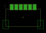
I am trying to create JST connector footprint of 6 pin smd , but i need to include 2 soldering pad on either side of the package. i try to place a pad for it, but while net listing error show up as extra 2 pad in the footprint.
kindly tell me how to go with the soldering pad which has no electric connection , which is only used for soldering purpose.
https://obrazki.elektroda.pl/7946715000_1404791306.png
https://obrazki.elektroda.pl/7946715000_1404791306.png
I am trying to create JST connector footprint of 6 pin smd , but i need to include 2 soldering pad on either side of the package. i try to place a pad for it, but while net listing error show up as extra 2 pad in the footprint.
kindly tell me how to go with the soldering pad which has no electric connection , which is only used for soldering purpose.
https://obrazki.elektroda.pl/7946715000_1404791306.png

https://obrazki.elektroda.pl/7946715000_1404791306.png


