Continue to Site

Welcome to EDAboard.com

Welcome to our site! EDAboard.com is an international Electronics Discussion Forum focused on EDA software, circuits, schematics, books, theory, papers, asic, pld, 8051, DSP, Network, RF, Analog Design, PCB, Service Manuals... and a whole lot more! To participate you need to register. Registration is free. Click here to register now.

Issue with Assura RCX

Status
Not open for further replies.

liuy1987

Newbie level 4
Joined
Jan 20, 2012
Messages
7
Helped
0
Reputation
0
Reaction score
0
Trophy points
1,281
Location
Dallas,TX
Activity points
1,332
Hi, I am using Assura to extract layout (pdk: tsmc35). In the layout, I have a transistor with width of 19.5u and finger of 10, the total width is 195u. But in the av_extracted view, I check the property of that transistor, and find its size is w=19.5u and finger=1, m=1. Then i did post-layout simulation with this extracted view, that transistor does function like a 19.5u-wide transistor. Can anyone tell me why? Why a 19.5u, f=10 transistor turn into a 19.5u,f=1 transistor after RCX?

P.S. DRC and LVS both pass.

Thanks in advance,
Yu
 

If your schematic view contains a W=195 transistor and your av_extracted view a W=19.5 transistor, it's hardly conceivable that LVS may succeed.
Are you sure that you compared the proper views?
 

Can you show either images of the 2 transistors in schematic and layout, or the respective lines from both netlists?
 

Can you show either images of the 2 transistors in schematic and layout, or the respective lines from both netlists?

Hi, thx for your reply. This is netlist from schematic:M0 (out _net0 0 0) nch l=350.0n w=7u m=10 ad=3.99e-12 as=3.5e-12 pd=9.54u ps=8u nrd=0.0714286 nrs=0.0714286
M25 (out _net0 vdd! vdd!) pch l=350.0n w=19.5u m=10 ad=1.1115e-11 as=9.75e-12 pd=24.54u ps=20.5u nrd=0.025641
nrs=0.025641
This is netlist from av_extracted view: M0 (_4\:eek:ut _1\:input 0 0) nch l=3.5e-07 w=7e-06 m=1 ad=3.5p as=3.99p pd=8u ps=9.54u nrd=0.0714286 nrs=0.121429
M25 (vdd! _1\:input _1\:eek:ut vdd!) pch l=3.5e-07 w=1.95e-05 m=1 ad=11.115p as=9.75p pd=24.54u ps=20.5u nrd=0.0435897 nrs=0.025641
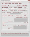
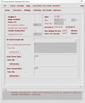
These are RCX parameters setting:
rcx1.JPGrcx2.JPGrcx3.JPG
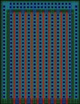
Layout of this transistor:layout.JPG
Property of transistor in schematic:schematic.JPG
 
Last edited:

Hi again,
thank you for all this info! Just a few ideas now:

1. I can't see if the 10 gates in your layout are connected -- but I'd suppose so.

2. Is it possible that your av_extracted view contains each 10 of these MOSFETS (M0, M25) with slightly different names (always with the same 4 nodes), totally widespread over the whole netlist -- and you just found one of them (each)?

3. If not, I'd suspect your extract rules aren't correct.

4. Also -- if 2. is not true -- your LVS shouldn't pass when comparing those two netlists. Then there would be something wrong with your LVS rules, too.

Both rules' sets corrupt? Rather unlikely! But then, I'm on my wits' end, sorry!

I checked the whole view, but there is only one transistor there. Even if I didn't find them, they should exist in the netlist, but not. Now i have to contact MOSIS for this issue. Thank you for your replies!
 

Now i have to contact MOSIS for this issue.

In order to demonstrate this I'd suggest to build an extra circuit, e.g. an inverter with M0 & M25 and run Assura and LVS. So the problem can be more clearly presented (and you get a better chance for their soon reaction).

If, however, these 2 transistors would get extracted correctly, you'd receive another hint (dependence on number of devices, hierarchy pb. ?).

Good luck! erikl

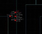
I tried that, but still failed to extract all the fingers. In the av_extracted view, symbol of transistor looks to have multi finger, but when I checked its property, it still have only one finger, and the same with netlist. Really strange.1.JPGproperty.JPG
 

In order to demonstrate this I'd suggest to build an extra circuit, e.g. an inverter with M0 & M25 and run Assura and LVS. So the problem can be more clearly presented (and you get a better chance for their soon reaction).

If, however, these 2 transistors would get extracted correctly, you'd receive another hint (dependence on number of devices, hierarchy pb. ?).

Good luck! erikl

I tried that, but still failed to extract all the fingers. In the av_extracted view, symbol of transistor looks to have multi finger, but when I checked its property, it still have only one finger, and the same with netlist. Really strange.View attachment 74275View attachment 74276
 

You could check your XTR rules and try and understand its syntax. Search for "fingers", e.g.

With our Assura extract rules, individual transistors (fingers=1 , m=1) were extracted for each layout finger.
Then only the LVS combined these individual transistors to a multifinger transistor.
For this, the LVS rules contained a parallel procedure for each device type, for MOSFETs e.g. something like:

Code:
procedure( parallelMOS(mos1 mos2)
let( ((l1 paramToFloat(mos1->l)) (l2 paramToFloat(mos2->l))
      (w1 paramToFloat(mos1->w (mos1->m||1.0)*(mos1->fingers||1.0))) (w2 paramToFloat(mos2->w (mos2->m||1.0)*(mos2->fingers|| 1.0)))
      (eqMos '(nil m 1) )
   )
   when( and(l1 l2)
      eqMos->l=min(l1 l2)
      when( and(w1 w2)
         eqMos->w=(w1/l1+w2/l2)*eqMos->l
      )
   eqMos->fingers = 1
   eqMos->m = 1
   )
   eqMos
))
 

Hi liuy1987,

I met the similar problem. In my case, after extraction, the netlist gives always finger=1, and width=(total width in schematic).
I wonder if you find explainations and solutions to get around for this?

Thanks.

jimiblues
 

Status
Not open for further replies.

Part and Inventory Search

Welcome to EDABoard.com

Sponsor

Back
Top