Continue to Site

Welcome to EDAboard.com

Welcome to our site! EDAboard.com is an international Electronics Discussion Forum focused on EDA software, circuits, schematics, books, theory, papers, asic, pld, 8051, DSP, Network, RF, Analog Design, PCB, Service Manuals... and a whole lot more! To participate you need to register. Registration is free. Click here to register now.

[SOLVED] Is this circuit correct?

Status
Not open for further replies.

d123

Advanced Member level 5
Joined
Jun 7, 2015
Messages
2,505
Helped
494
Reputation
992
Reaction score
525
Trophy points
1,393
Location
Spain
Activity points
27,148
Hi,

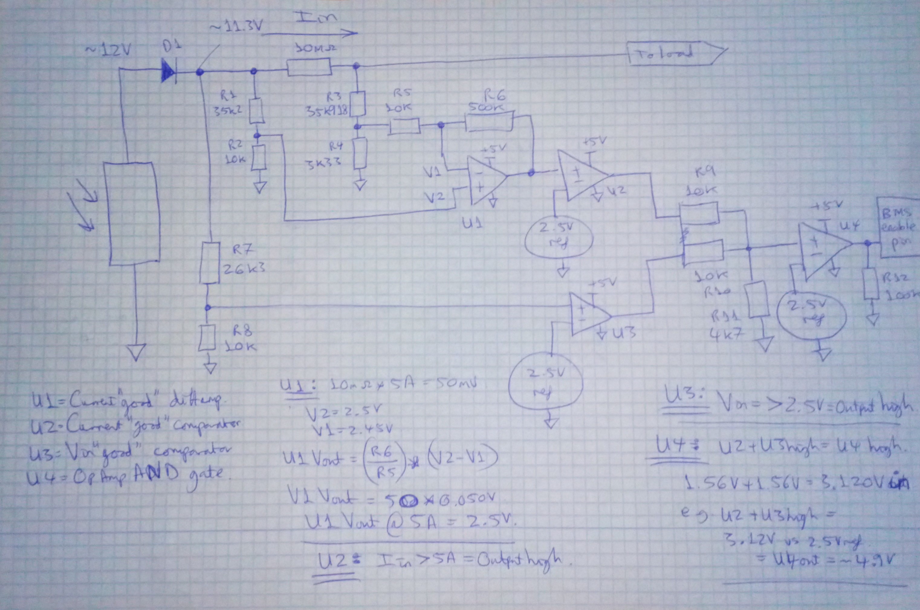
Suggested a circuit to a person on another forum, did it in a hurry and made an ass of myself as usual by making a silly mistake with the difference amplifier common-mode range when the OA is on a lower supply voltage to the PV panel voltage. I have tried to correct it myself by reasoning out that section, but I'm not certain if the solution is functionally correct by dividing down V2 and V1, then multiplying the V2 - V1 result by 50.
It's the voltage divider into Vin- feeding into the gain section of 500k/10k that I'm most unsure of.

1) Can someone say whether the difference amplifier section is correct for 5A across 10 mOhm resistor = 50mV across U1 Vin+ to Vin- = 2.5Vout. Not precise microvolt, just correct to a few mV or so. And that the common-mode range of U1 won't be violated?

As a 'rough sketch' circuit, can the whole thing work as desired, and at 5V op amp supply?:

1 Diff. amp: >5A across Rsense= >2.5V out
2 Current good: >5A = >2.5V ref = U2 high
3 Voltage good: >11.3V in = >2.5V ref = U3 high
4 AND op amp: U2 (= ~4.9V) + U3 (= ~4.9V) = U4 high (~4.9V out)
5 BMS enable pin

In other/less words:
1 > 50 mVin = 2 high
2 high + 3 high = 4 high
4 high = 5 high

Thanks.
_20201027_181803.JPG
 

I would advise you consider an integrated IA to do this, because
of the small signals involved, the high CM environment, and need
to get precision Rs to produce good CMR. Just a thought. These
are laser trimmed on production line to produce good performance.


Here is an analysis that shows just how sensitive CMR is to amp to amp G
variations and fdbk factors (resistor ratios).

1603894107419.png


Regards, Dana.
 

Attachments

  • CMR Analysis IA.pdf
    170.7 KB · Views: 127
  • Like
Reactions: d123

    d123

    Points: 2
    Helpful Answer Positive Rating
Hi Dana,

Thanks, good reminder of how bad discrete difference amplifiers are... I'll read those, I was reading about difference amplifiers again earlier. I have a couple of INA826s, but the circuit isn't anything I'm going to need/make for the timebeing, maybe, never say never.

I breadboarded the difference amplifier section yesterday, horrible. Simulated the same circuit today, equally horrible. At least the real and simulated results were equally awful and matched calculations about the simpler parts I wanted to check.

Would you happen to know why the INA826 evaluation module app. note uses a bypass capacitor to ground on the V- pin (gnd pin) for a single supply circuit? I understand why on a dual supply, but not on a single supply, I can intuit it's either a copy/paste typo or to keep noise away from gnd pin but not sure how that works... I was re-reading earlier about decoupling/bypassing but found nothing similar, vague references to the practice at best, and mainly only well-known capacitor from V+ pin to gnd or the capacitor across V+ pin and gnd pin, the typical configurations.

Screenshot_20201028-202346.png
 

Attachments

  • sbou115c.pdf
    438.6 KB · Views: 110

Hi,

There are "high side current sense amplifiers" they are optimized for this application .... and usually cheaper than INAmps.

Klaus
 
  • Like
Reactions: d123

    d123

    Points: 2
    Helpful Answer Positive Rating
The schematic I think is trying to show either terminate to V- with bypassing or just
to ground. The pic is confusing.

1603925343941.png


Those two amps not running open loop are they ? I dont see any fdbk around them....
If thats the case they would function not as amps buts a s comparators.


Regards, Dana.
 
Last edited:
  • Like
Reactions: d123

    d123

    Points: 2
    Helpful Answer Positive Rating
R1 to R4 need to be very accurate and zero drift if the circuit in post #1 is to work reliably - often this is not the case - so that circuit is never used for original signals < 100mV .....
 
Hi Dana,

The schematic I think is trying to show either terminate to V- with bypassing or just
to ground. The pic is confusing.

Okay, thanks.

Those two amps not running open loop are they ? I dont see any fdbk around them....
If thats the case they would function not as amps buts a s comparators.


Regards, Dana.

Yes, they are being used as comparators.
--- Updated ---

Hi Easy peasy,

R1 to R4 need to be very accurate and zero drift if the circuit in post #1 is to work reliably - often this is not the case - so that circuit is never used for original signals < 100mV .....

Not only the worst version of the three discrete difference amplifier configurations I'm aware of, but also a 25mV to 50mV signal, <<100mV. Thanks for explaining that aspect, very useful to know.
--- Updated ---

Hi Klaus,

Hi,

There are "high side current sense amplifiers" they are optimized for this application .... and usually cheaper than INAmps.

Klaus

That's a very good point, thank you. I still have one INA286 left, the 200V/V.

Thanks.
 
Last edited:

Hi,

I doubt that the input voltage at U4_+IN is correct. Please run a simulation.

The problem with the INA is not only the INA itself, it´s the high precision resistors your need. And even if you use a pot for calibration I expect thermal runaway. A high gain of 200V/V makes things worse. In the end it depends on your requirements/specifications whether the circuit is useful or not.

And I don´t like the "mistreating" of an OPAMP as comparator.

Klaus
 
Hi Klaus,

Hi,

I doubt that the input voltage at U4_+IN is correct. Please run a simulation.

You are correct, in fact not only that one but also several of the other voltages are wrong. In fact, the circuit is far worse than I'd even expected. I simulated it for your benefit (and mine) to confirm your observation and included as many signals as possible in the transient results, I had to omit a few signals that seemed less interesting (or should be obvious) than those included as they didn't all fit into the little window. This circuit is so badly-designed because of rushing the idea it's an embarrassment, funny but one to be ashamed of. I didn't even consider that 5A*1R = large voltage drop so two resistive dividers are wildly wrong. I hope you find the simulation results as amusing as I have.

The problem with the INA is not only the INA itself, it´s the high precision resistors your need. And even if you use a pot for calibration I expect thermal runaway. A high gain of 200V/V makes things worse. In the end it depends on your requirements/specifications whether the circuit is useful or not.

And I don´t like the "mistreating" of an OPAMP as comparator.

Klaus

Oofff, you mentioned the word trimpot in the same context as a precision circuit, it sent a horrible shiver down my spine just at the thought of it.

Do you mean a proper manufactured instrumentation amplifier like the INA826 or a discrete version or the INA286 current shunt monitor IC? The INA 826 in amp has the high precision resistors in the IC package, you 'only' have to provide the gain resistor.

I still have one INA286 waiting to be used as the 200V/V gain is hard to factor in to many of my little circuits - it usually ends up having a higher Vout than my supply voltages so I never use it as I have as the lowest value, 5mOhm current-sensing resistors, that or 3 mOhm to 7 mOhm '0' Ohm resistors.

Op amp comparators were to make full use of a quad package, and even the LMC6464 datasheet shows it used as a comparator, but I understand what you mean - it is not the best approach if a comparator IC is available.

Looking at the transient results, all that is missing is that well-known sound of pathetic failure: Waaaah, waaah, waaah...

VGOOD IGOOD CIRCUIT V1 BAD CIRCUIT.JPG
 

Hi,
I simulated it for your benefit
No need to do it for me ;-)

Oofff, you mentioned the word trimpot in the same context as a precision circuit, it sent a horrible shiver down my spine just at the thought of it.
They are often used. But they need the correct circuit. In your case moving from one side to the other should vary the "offset" just about a millivolt or so.

I meant the current shunt monitor. This is what I recommend to use.
Honestly I didn´t open the datasheets. I was mislead because "INA" often is used as an abbreviation for common "Instrumentation Amplifiers".

Mind the kelvin wiring at the miliiohms shunts.

***
Some thoughts:
* Is the "voltage good" threshold correct? It seems to be used for a 12V signal, but the threshod level is at 9V. And shouldnt it sense the voltage of the PV? means at the ANODE side of the diode?
* I recommend to use positive feedback at the comparators .. just to get clean edges without chattering.
* you may omit R11... and replace R10 with a (schottky) diode (cathode to U3). --> less components but improved voltage levels.


Klaus
 
Your OpAmp diff amp circuit has unbalanced Gs in the inverting and non-inverting
paths, so is not rejecting CM.

Here I just tied the two inputs together and swept the input to see what the CM rejection
was with your R values. As you can see there is NO CMR from the circuit, so that swamps
out the contribution of the tiny shunt V.

1603970910441.png


here is a typical G of 10 circuit with Rs -

1603971121572.png


Regards, Dana.
--- Updated ---

Heres a sim with shunt and correct CMR -

1603972783248.png


Regards, Dana.
 
Last edited:
Hi Dana,

Your OpAmp diff amp circuit has unbalanced Gs in the inverting and non-inverting
paths, so is not rejecting CM.

Here I just tied the two inputs together and swept the input to see what the CM rejection
was with your R values. As you can see there is NO CMR from the circuit, so that swamps
out the contribution of the tiny shunt V.

Regards, Dana.

Thanks, nice to see a correct version of the diff. amp! I read that yesterday about common-mode and differential, that the problem (...one problem...) with that configuration is that 1/2 (V1 + V2) will appear at the output as well as the product of V2 - V1. It explains the ~1.8V that puzzled me.
--- Updated ---

Hi Klaus,

Hi,

No need to do it for me ;-)


They are often used. But they need the correct circuit. In your case moving from one side to the other should vary the "offset" just about a millivolt or so.

I meant the current shunt monitor. This is what I recommend to use.
Honestly I didn´t open the datasheets. I was mislead because "INA" often is used as an abbreviation for common "Instrumentation Amplifiers".

Mind the kelvin wiring at the miliiohms shunts.

***

I thought you might find its pathetic-ness amusing.

Okay. Offset nulling.

'Funny' code, INA, I suppose it's because it's similar to an in amp, maybe?

imagen_2020-10-29_140827.png


Some thoughts:
* Is the "voltage good" threshold correct? It seems to be used for a 12V signal, but the threshod level is at 9V. And shouldnt it sense the voltage of the PV? means at the ANODE side of the diode?
* I recommend to use positive feedback at the comparators .. just to get clean edges without chattering.
* you may omit R11... and replace R10 with a (schottky) diode (cathode to U3). --> less components but improved voltage levels.


Klaus

There's no need to rub it in ;)...

Yes, that threshold is/would be correct, except for the voltage drop when the load draws 5A. Idea was not to trigger comparator until PV had reached 9V and Iout 5A. Sigh... It senses at the diode cathode side to include the diode voltage drop.

Okay, I know how to calculate hysteresis and centre trip-point around Vref, but this was a rough-and-ready quick circuit.

That's a new one for me about the Schottky diode, thanks for the tip.
 
Last edited:

Status
Not open for further replies.

Similar threads

Part and Inventory Search

Welcome to EDABoard.com

Sponsor

Back
Top