Continue to Site

Welcome to EDAboard.com

Welcome to our site! EDAboard.com is an international Electronics Discussion Forum focused on EDA software, circuits, schematics, books, theory, papers, asic, pld, 8051, DSP, Network, RF, Analog Design, PCB, Service Manuals... and a whole lot more! To participate you need to register. Registration is free. Click here to register now.

Is this circuit connection is right in advance design system?

Status
Not open for further replies.

noor84

Member level 5
Joined
Dec 27, 2017
Messages
90
Helped
0
Reputation
0
Reaction score
0
Trophy points
6
Activity points
688
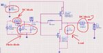
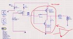
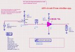
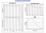
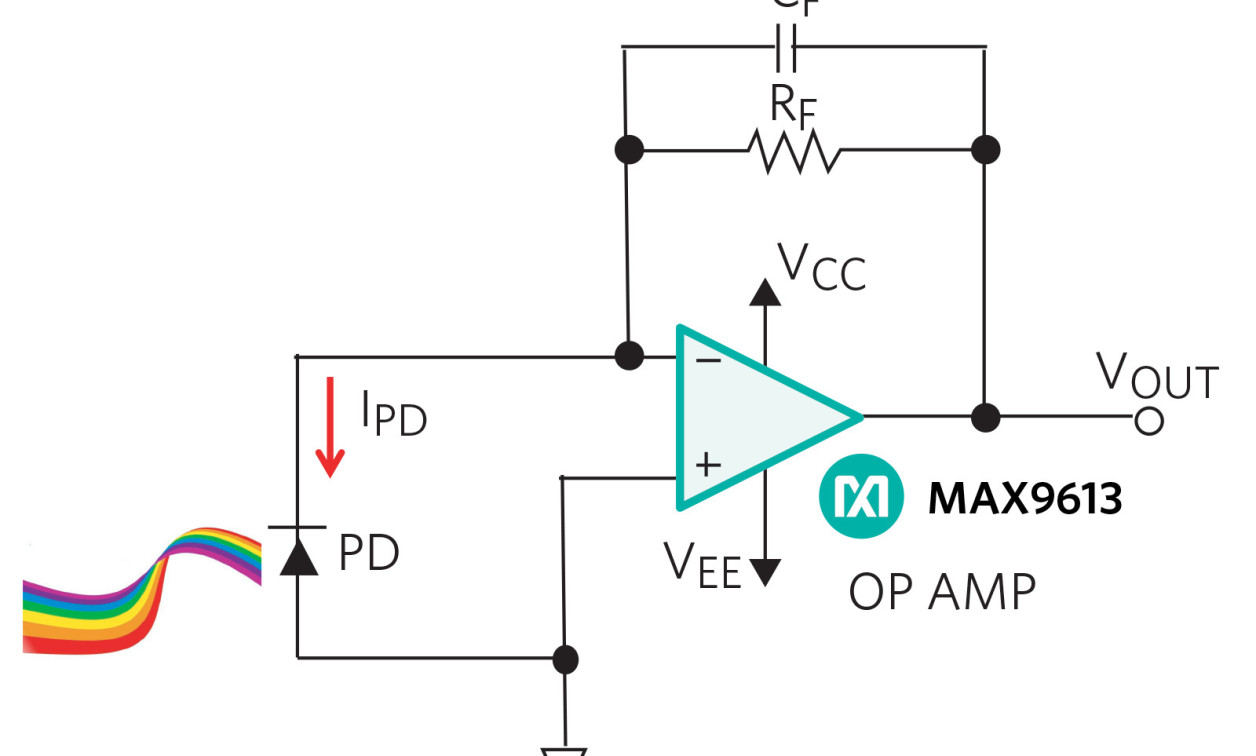
I want to make a simulation of Transimpedance amplifier circuit to measure the dB(TIA)and voltage gain using Advance Design System(ADS simulator).
Please, may you advise me if my circuit connection(in attachments) is right or not?

e.jpg
 
Last edited by a moderator:

-Term2 will load the circuit in regard of DC.Place a coupling capacitor.
-How DC Current Source (SRC4) will sink the current ?? Nonsense,..
-Your circuit is not Current Controlled, Voltage Controlled B-Class... It won't work..
 

-Term2 will load the circuit in regard of DC.Place a coupling capacitor.
-How DC Current Source (SRC4) will sink the current ?? Nonsense,..
-Your circuit is not Current Controlled, Voltage Controlled B-Class... It won't work..


Dear BigBoss,
Many thank you for your the advise,
I attached new pic with DC coupling capacitor.
Please, any solution for DC Current Source (SRC4) to sink current?
 

Attachments

  • e1.jpg
    e1.jpg
    159.6 KB · Views: 86

Place an Ideal Inductor between supply line and Current Source so that the Current Source will able to sink its current.
But there are still configuration errors.. This circuit is not current controlled.
Photo Diode will drive a circuit by its current so when the light is dark, the current will be very low, when the light is bright, the current will flow into circuit.The configuration must be so to my knowledge.. Because Transimpedance means
\[ Z_{imp}=\frac {V_{out}} {I_{in}} \]

So, the Input will be Current, the Output will be Voltage. But your Input ?? The Input Current cannot flow into MOSs' Gate..


Dear BigBoss,
From your knowledge, is my circuit cannot measure the value of transimpedance amplifier?
I made a change on the connection of the previous circuit and I attached it in the attachments(named my circuit).
This connection is taken from a connection can be found it in the wire-line App. in the design guide of ADS. the picture name( ADS circuit) in the attachments.
The results of the ADS circuit in the attachments.
So, can I depend on this circuit as I connected my circuit in the attachments(named my cct) to simulate and measure the Z(TIA) and gain.....etc?
Thank you in advance.
 

Attachments

  • my cct.jpg
    my cct.jpg
    203.3 KB · Views: 84
  • ADS circuitpng.jpg
    ADS circuitpng.jpg
    149.8 KB · Views: 82
  • Results.jpg
    Results.jpg
    134.4 KB · Views: 78
Last edited:

The basic circuit is a self biasing amp consisting of the N and P
MOSFETs, using R1 as source of DC and AC fdbk. It does function as
a TIA when current is passed thru R1, the output will be a V with
a G determined by MOSFET parameters and loading.

R1 nominally fairly high in value to produce adequate G for low currents
from photo diode.


https://www.analog.com/en/products/...ifiers/optical-transimpedance-amplifiers.html ap notes here as well

Note that relying on biasing from MOSFET Vth's is a poor solution as device to device variations
in Vth will cause the simple stage to bias up at significantly different bias points. Also bias
point very T sensitive due to Vth dependency on T. Also to get adequate G R1 wants to be large,
which is counter to speed, as always trade offs.....

Then nominally you want an AGC loop of some sort to manage the T & V dependencies of the
amplifier.


Regards, Dana.

Dear Dana,
Thank you for your reply,
I know the idea of the principle of how TIA work.
My problem is how can I measure the value of (gain ITA, input referred noise, ...etc) using Advance design system (ADS).
Please, I wrote message to BigBoss about the measurements, could you please read my message that I wrote it in the above?
Thank you in advance.
Regards.
 

Status
Not open for further replies.

Similar threads

Part and Inventory Search

Welcome to EDABoard.com

Sponsor

Back
Top