Continue to Site

Welcome to EDAboard.com

Welcome to our site! EDAboard.com is an international Electronics Discussion Forum focused on EDA software, circuits, schematics, books, theory, papers, asic, pld, 8051, DSP, Network, RF, Analog Design, PCB, Service Manuals... and a whole lot more! To participate you need to register. Registration is free. Click here to register now.

Is there a way to use/run more than two variables simultaneously in Cadence?

Status
Not open for further replies.

Osawa_Odessa

Banned
Joined
Dec 31, 2012
Messages
168
Helped
1
Reputation
2
Reaction score
1
Trophy points
1,298
Activity points
0
Hi,
Is there a way to use/run more than two variables simultaneously in Cadence?

I need to run DC simulation for cascode power amplifier with three variables simultaneously to choose values with maximum transconductance, gm max.
Three variables are:
+ Vbias: Vgs
+ n1: number of finger of the first transistor.
+ n2: numberr of finger of the second transistor.

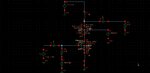
Here is the schematic:
 

Attachments

  • cascode 2.jpg
    cascode 2.jpg
    91.6 KB · Views: 115
Last edited:

Hi,

You can run parametric analysis in ADE L window... for sweeping more than 2 variables.... but it uses combinations of all three parameters ...

Thanks...
 
Thanks, I have just discovered that. In parametric analysis, I can use up to 4 variables. What did you mean by "it uses combinations of all three parameters"?

- - - Updated - - -

I have just run three variables above for Id (drain current). To compare and choose Vgs, n1, n2 I need to plot all transconductances gm and choose the best one. This is really difficult because there are two many Id and so I need to plot all gm from them. Finally, choose the ones with best gm. This require a lot of effort and take a lot of times. Is there other ways to do this easier?
 

Do yo really mean 1k (1000H) source inductance? :lol:
 

Is there other ways to do this easier?

Try the Optimization tool:
Optimization-tool.gif Here comes the User Guide.


Do yo really mean 1k (1000H) source inductance? :Laughing:

I think this is just for total isolation of the cascode transistors from external elements, in order to get the unaffected gm simulation values.
 
The inductor works as a constant current source for AC, effectively cancels M0 gm and leaves only Cgd as signal path.
 
Right! The ac source (V3) should be attached to the source of M0, not to gnd.
 
Thanks, I have just discovered that. In parametric analysis, I can use up to 4 variables. What did you mean by "it uses combinations of all three parameters"?

Hi,
Actually it runs for every single combination of the variables... ex Id = 100u n1=1 n2 =1 then id=100u n1=2 n2 =1.. like this and you get many outputs ... you can try what "erikl" said.. optimization tool..

Thanks
 
You can also use Ocean and bring results back into the
ADE, which would let you mess with variables any way
you'd like (for example, making "cases" of variable combos).
Use the ADE to create the starting Ocean deck w/ all
the settings and saved-outputs etc. and modify it from
there.
 
Thank you, everyone, for helps. I am learning to use optimization as you suggested. I am new to Cadence and this is the first time I know this kind of simulation.
Right! The ac source (V3) should be attached to the source of M0, not to gnd.
I don't understand why it is so. This schematic is from a paper in IEEE and I am following the paper.
 

Thank you, everyone, for helps. I am learning to use optimization as you suggested. I am new to Cadence and this is the first time I know this kind of simulation.

I don't understand why it is so. This schematic is from a paper in IEEE and I am following the paper.

Hi,

May be the act of inductance as a constant current source introduces infinite resistance .. so it vanish the acutual transistor gm.. so that he suggested to do that.. i think.. try two methods and find the difference and let us know..

Thanks

- - - Updated - - -

Hi,

Is there optimization option for cadence virtuoso IC 6.1.5.72..

Thanks
 

This schematic is from a paper in IEEE and I am following the paper.
What's the Ls value assumed in the paper. I gues nH range or below.
 

Hi,
The paper didn't specify any component values, therefore, I am confused about what should I choose. I read about common source degeneration in which it said that Ls is arbitrarily chosen and then Cgs (capacitance between gate and source) is specified based on Ls. My confusion is why we can choose Ls arbitrarily? This means that Cgs is also can be arbitrarily chosen, that seems not right.
 

If you mean to integrate the inductor on-chip then
Q, current and area will limit your range of choices
quite a bit. L is the big area driver in the narrowband
PA layouts I've seen, and will be until at least X-band.

"Arbitrarily" works on paper. It never holds up all the
way to tapeout.
 

Status
Not open for further replies.

Part and Inventory Search

Welcome to EDABoard.com

Sponsor

Back
Top