Continue to Site

Welcome to EDAboard.com

Welcome to our site! EDAboard.com is an international Electronics Discussion Forum focused on EDA software, circuits, schematics, books, theory, papers, asic, pld, 8051, DSP, Network, RF, Analog Design, PCB, Service Manuals... and a whole lot more! To participate you need to register. Registration is free. Click here to register now.

IRF450 MoSFET

Status
Not open for further replies.
You can see as Vgs rises the device turns on and allows, as Vgs increases, progressively
more current (Id) thru it -

1651244447025.png


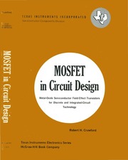
Here is a pretty good book on MOSFETS -


Regards, Dana.
 
Last edited:

IRFxxx Mosfets have an input threshold voltage Vgs(th) from +2V for some of them to +4V for some of them when they barely begin conducting an Ids of 0.25mA. They need a Vgs of +10V to fully turn on.

IRLxxx Mosfets have a lower input threshold voltage (Vgs(th) from +1V to +2V and need a Vgs of +5V to fully turn on.
 
Hi,

you give a link to a datasheet, but not directly to the manufacturer.
I always recommend to use the datasheet from the manufacturer. Also visit the manaufaturer´s product page.
There you find most up to date informations about the device .. and also additional informations like application notes, design notes, availability ... and so on.

BTW:
The usual way when developing a circuit is the other way round.
--> first you have the requirements for the MOSFET then you choose a MOSFET.

Besides Dana´s recommendation:
go to youtube, do a search for "how MOSFET works" (or similar) and watch a couple videos.

Klaus
 

I might be able to help on this topic as it is one of my engineered part.

1. IRF has been part of Infineon since 2016. Your parts datasheet is http://www.irf.com/product-info/datasheets/data/jantx2n6770.pdf

2. The n channel power MOSFET is switched on by applying a positive voltage on its gate terminal. According to its datasheet, the threshold voltage is 2-4V. So, you could put a 3V on gate. Said gate rating is called Logic Level, LL.

3. But a voltage does not turned it ON, untill its gate is fully charged. Charge = Current x time. In order to get the rated current level, you have to fully charge its gate, says Qgs and Qgd. The later one, Qgd, represents the switching performance of this part, which contribute to the switching loss as well. One have to charge the gate to turn the MOSFET on, and discharge it to turn it OFF.

Should you need any further assistance please reply this comment. Hope it helps.
 

The n channel power MOSFET is switched on by applying a positive voltage on its gate terminal. According to its datasheet, the threshold voltage is 2-4V. So, you could put a 3V on gate.
Absolutely not!
Some of them conduct only 0.25mA (250uA) when the gate-source voltage is a threshold voltage of only 4V then they will conduct even less at 3V. The datasheet guarantees that all of them conduct well (with a low on-resistance) when the Vgs is 10V.
 
Absolutely not!
Some of them conduct only 0.25mA (250uA) when the gate-source voltage is a threshold voltage of only 4V then they will conduct even less at 3V. The datasheet guarantees that all of them conduct well (with a low on-resistance) when the Vgs is 10V.
Please be aware the gate rating represent the gate oxide thickness that could withstand the maximum Vgs voltage. It does not correlate to the threshold voltage.

Today, to maximise the cost - Rdson, manufacturers reduce the gate oxide thickness. For logic level, Gox used to be 30-40nm (1150degC Nitrigen oxidation process). But now, it is getting thinner, thinner and thinner, using RTA or laser oxidation, high energy implant, etc. Further, to further reduce Rdson, manufacturers layout their device along 110 wafer orientation instead of 100, resulting oxide integrity degradation.

For example, please test aforementioned MOSFET in curve tracer using square signal and your might find a dimple at +1-+2VGgs, which is a phenomenon of said gate rating. The root cause attribute to its process - LOCOS caused a bird beak at the GOX trench corner, where GOX is much thinner due to the N in the LOCOS process. The phenomenon is reported by a Dutch engineer decades ago, and hence discussed here.

There are several approaches to circumvent said issue, of which some were classified as commercial secret. You could ask the manufacture why they do not use some advance tech, but they keep silence...

Therefore, to ensure the device reliable and durable, please be careful to the gate rating. Should the client wish to apply a higher voltage on the gate, please check the datasheet, or ask manufacture, or do a gate oxide breakdown test, Vgso and Vgdo. Of course, ESD add on is another story.
 

Hi,

I agree with @Audioguru.

The datasheet says: V_GS_TH = 2...4V for a tiny current of 250uA.
This is not considered as ON state for a switch.

@danadakk gives good information about: the behviour between a load and switch.

But - in opposite to a regulator - a "switch" always is overdriven to ensure low ohmic Drain-Source even at worst case condition. (temperature, production tolerance... )
No good designer will drive the IRF450 as a "switch" with only V_GS = 4V... and using 3V makes no sense at all. ... even if the load current is below 0.001A
(it also makes no sense to use a 13A rated MOSFET for only 0.001A load current)

Klaus
Hi Klaus

Do agree with your suggested 4V. But for 10Vgs indicated by Audioguru, I hesitates. Perhaps for consumer electronics, 2-3 year lifetime, it works. But for automotive MOSFET, the concern is raised on its durability. You might find the identical MOSFET in said manufacturer automotive catalogue but the gate rating is degraded to 8V, 6V or even lower.

No offensive, I remember those old time when IRF CEO Alex visit his customers and raise MOSFET price by 30%. You know, everyone try to design out IRF parts. IRF played very similar game in its device inside as well. Its datasheet claims logic level but its gate oxide is only 26 nm. Its marketing manager thought the customer is more likely to find the device wear out rather than do a FIB SEM inspection to diagnose the root cause failure (GOX breakdown).

Today, a well know electric drill does not last for 5 year, because they asked the manufacturers to control the lifetime to 2 year. For cost down, the manufacturer used Schottky -MOSFET instead. As we all know that Schottky body diode trade off lds leakage for Rdson and Trr. The consequence is the extra power consumption in the standby mode, and the degradation of the gate oxide. A end user wont recognize it leads to rapid discharged battery until the drill wear out in a few months when the 2 year warranty period expired.

Please check the datasheet of said electric drill MOSFET, its 250uA or 100uA current rate does not exceed. But, is the MOSFET really switched on at 0.25mA. One should define the threshold voltage at the peak of transconductance. In the datasheet, it should be termed as the current density. But, there is no die size mentioned on datasheet, as related to the cost. On the other hand, 250uA Ids is predominately dependent on test and die size. The person who manipulate the datasheet is unlikely to know where and how the 250uA comes from. Should you be interested, you could look into a MOSFET device and try to measure its Ids from active cell, edge termination, and perhaps the leakage current (pA range). The edge termination does also contribute to Ids in particular for a a large die. Please try to completely turn off the device, perhaps by applying a negative voltage on its gate, you might still observe the Ids. It is mainly contributed by the edge. You could find the drain terminal on the die front surface. The leakage current is mainly attributed by the insulate material. Before TI acquire cyclon, its lateral power MOSFET is highly leaking because of poor gate oxidation process.

You are absolutely right, that temperature does affects the threshold voltage. There is no industry standard in the datasheet threshold voltage test. Each manufacture define its own way as to sale its MOSFET. You might teardown the MOSFET in apple iphone has no datasheet. The physical mechanism of the temperature affected Vgst is studied by few companies. Most manufacturers do not will to invest to know how but for shrink the pitch for cost. Most datasheets in market were written by marketing guy who knows nothing about the Vgst, temperature, process variation, DOE, 6 sigma, etc.

For example,

1. you could get the sample from 10 suppliers for the same Vds and Ids rated MOSFET, and please test its BVdss, you might find the 5%-10% higher BVdss measured on US or EU suppliers. 10% for Asian players, Hitachi / Panasonic was 30%. You might observe their test method varies, in some case varies a lot.

2. measure the 250uA Vgst in said 10 devices, you might get Vgst close to 2.4-2.8 for well known players. But their Rdson curves varies a lot.

3. Compare the 75degC and 25degC Vgst curve, you might find significant discrepancies with the datasheet for at least 7 suppliers.

You know much more than in the circuit /PCB design, and certainly I was teaching grandma how to suck eggs. However, there is something, e.g. physics, cannot be bended. It is possible to get low Rdson, Cgd, Trr, or two of them (FOM - Figure of Merit), but not all of them.
 

Korean, you talk of how Mosfets are made today and you talk about Vgs breakdown.
The IRF540 Mosfet is OLD and has a Vgs breakdown rating of 20V but its datasheet shows that it works well with a Vgs of 10V.

The IRL540 Mosfet is newer but is still so old that it is almost obsolete. It has a Vgs breakdown of 10V and it works well with a Vgs of 4V and 5V.

The curves on a datasheet are for devices that have "typical" specs, not for many devices that have minimum and maximum specs.
Howdo Audioguru

Really appreciate your reply and I am sorry that my concern focus on the reliability. I agree with you that for a Vgs 20V rated device 10V or 20V is acceptable. Because 20V represent standard level device, not logic level, its gate oxide thickness is above 65nm. For IRF part, its targeted standard level GOX thickness is 72nm. So theoretical breakdown voltage is above 70V. I am sure one could put a 60V on its gate but not for long.

Further, typical value on the datasheet is commonly a marketing behavior. You could purchase two parts from its consumer and automotive catalogue respectively. Two different Vgst typ spec on datasheet, but identical same electrical characteristics. Of course the price is much higher for the automotive one. When you ask why they sale the same device for different price, they would told you that the automotive one has extra reliability design and process. IRF, is now part of IFX, who have 100% tested their products (on wafer and assembly). There is no difference in the wafer process, assembly, and test. The difference is made on the datasheet.

We know the technology and love it. The datasheet is however written by a marketing guy or assigned application engineer, who spend all their time to analyze us - the customer. One thing they dislike or even hated, is the our discussion. We share our knowledge and know how, which lead to a transparent price and profit - cut their bonus from 8% to 0.5%.

Were you a marketing manager of a manufacturer and read this thread, you wonder why and how I know these fact. Let me be frank with you that I started from cleanroom, fabricate semiconductor, qualify it and research it. 800 parts in different manufacturers have been failure analyzed on my hand. I know its technology, its process, its cost. I manipulated 200 datasheet, SPICE models and even build a excel VBA program to build thermal impedance model for a manufacturer. Acting as marketing manager, my team designed in mosfet for an high volume automobile customer. Even work for said automobile customer to qualify another supplier as second source. To squeeze the extra profit in technology, I designed the thermal dissipation package for a PCB company in EU and then coincidently joined a well known electronic giant as procurement consultant, reducing millions of cost pre year for said client.

As circuit designer or end user, we play with the device itself, not the datasheet. Put a 40V datasheet MOSFET on curve tracer, and it might be 43V-48V. Please do not be surprised that it might give 56-65V, since that datasheet was written by marketing guy who has successfully turned scratched lots or unwanted stock into profit.

Recently I tried to fix a stereo system for one of my neighour and joined this forum. Lack of knowledge in the audio amplifier, I asked all your experts to spot out the signal input port on that PCB. Looking forward to your elegant advice and support. Thanks in advance.
 

Korean, ‘Brevity is the soul of wit’.

Nobody has the time, or inclination, to read your interminable, self-congratulatory diatribes. Not sure what your point is, but you should understand that chips ( or capacitors, resistors, etc.) can go through screening processes to qualify them for commercial, or automotive, or military, or space application. They may all very well come from the same fab, but the screening is what differentiates them, not necessarily the fab process.
 

Status
Not open for further replies.

Similar threads

Part and Inventory Search

Welcome to EDABoard.com

Sponsor

Back
Top