Continue to Site

Welcome to EDAboard.com

Welcome to our site! EDAboard.com is an international Electronics Discussion Forum focused on EDA software, circuits, schematics, books, theory, papers, asic, pld, 8051, DSP, Network, RF, Analog Design, PCB, Service Manuals... and a whole lot more! To participate you need to register. Registration is free. Click here to register now.

ir2110 heating issue

Status
Not open for further replies.

assu

Junior Member level 3
Joined
Dec 8, 2011
Messages
28
Helped
0
Reputation
0
Reaction score
0
Trophy points
1,281
Location
PAKISTAN
Activity points
1,508
Salam to all
I m using the following ckt with my buck converter the issue is the ir2110 heats up after 3 seconds...i have tried two ckts but it doesnt matter it still heats up .
Can anyone tell me what is the issue?
Note: 15Vdc is from solar pannel. N-channel mosfet is used for high side.

2rq1r11.jpg

cjfrp.jpg
 
Last edited by a moderator:

Do you have current probes to check VxI transition power or monitor with 100mV current shunt?

1st case with diode improves fall time and improves Mosfet transition losses at the expense of higher driver current losses.

Is boost voltage in range?
 

I m using the following ckt with my buck converter the issue is the ir2110
Hi
You sure you have used IR2110 ? you schematic says it is IR2101 isn't it ? if you used IR2110 i must say that can't operate as a bootstrap drive in the position which you've used . it must have L side too . but if it's IR2101 everything is different .
So what you have done ?

Best Wishes
Goldsmith
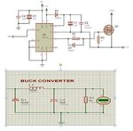
 

its ir2110 as i haven't got the model of ir2110 so couldnt use it to draw the schematic, in real i have made the ckt with ir2110.
So ir2110 cannot work only as high side , it should also have the low side too?
Hi
You sure you have used IR2110 ? you schematic says it is IR2101 isn't it ? if you used IR2110 i must say that can't operate as a bootstrap drive in the position which you've used . it must have L side too . but if it's IR2101 everything is different .
So what you have done ?

Best Wishes
Goldsmith

ir2110 is my first interaction to use the ic to drive MOSFET as i have never had driven mosfet through ic's.
i personally dont have current probs but i will check the lab in my university.
the boost voltage Vb is 15Vdc
reference picture from where ckt is obtained
buck.jpg
Do you have current probes to check VxI transition power or monitor with 100mV current shunt?

1st case with diode improves fall time and improves Mosfet transition losses at the expense of higher driver current losses.

Is boost voltage in range?
 
Last edited by a moderator:

I am having the same problem but I am using a hip4081 full h bridge it may be unrelated yet ironic so I will post a new thread but also looking at this one.
 

Hi,

I see two points:
1) the lefthand side of the bootstrap diode needs a capacitor. In my eyes it should be way larger than the bootstrap capacitor (10 ×)
2) are you aware, that the bootstrap circuit needs a low ohmic connection to Gnd in times to charge the bootstrap capacitor. Therefore you must not work with 100% duty cycle. At least every some ms you need a low for some us.

Klaus

Added:
To improve on this you may use the LO pin to drive the HS pin to GND. Maybe you need extra circuit on driving LI synchronous to HI. When HO is low, then LO needs to be low too. Avoit crossconducting..

Good luck
Klaus
 
Last edited:

I agree to the points about possible problems with bootstrap driver for asynchronous buck converter. Operation will fail without load current or with duty cycle near 100 percent. But the problem doesn't explain the reported "heating" of the IR21xx driver. There must be a different problem, e.g. massive undershoot of the switching node due to unsuitable circuit layout. It can kill a bootstrap driver, please review the respective IRF application notes.

We also don't know the actual application circuit, there may be other problems e.g. wrong IR2110 wiring, although IR2110 can be used for high-side only circuits.
 

Hi,

... yes, the overheating problem.

I can imagine, that because of the missing capacitor at V+ and combined with the pulses caused by bootstrap charging there are voltge spikes (positive and negative). Maybe this causes additional current inside of the driver.
Usually the power dissipation of the driver is low and there are only some degree celsius in temperature rise.

Oh, the drain of the FET is on the same line, so switching of the load causes extra voltage spikes.
Now i recommend to use a 10 Ohms series resistor to V+, a ceramic 100n and a 47U tanatalum.
Also i recommend a LOW ESR electrolytic capacitor at drain of FET, at least 100uF (up to 1000uF), paralleled a 100nF ceramic.
An overvoltage protection on V+ with an external 20V zener may also improve functionality.

Hope this helps
Klaus
 

Hi,
Added:
To improve on this you may use the LO pin to drive the HS pin to GND. Maybe you need extra circuit on driving LI synchronous to HI. When HO is low, then LO needs to be low too. Avoit crossconducting..

Good luck
Klaus
Well i am not using 100% duty cycle, i m driving it on 39% duty cycle.
By the above statement u mean to short the HI AND LI TERMINALS so the PWM that is being fed is same to both of them.??
also please be sure that i only want to use the high side not the low side
 

HI,

do you know how the bootstrap works?

You have to ensure, that the VS pin is low ( at least for some us) to charge the bootstrap capacitor.
Either the load ensures that, or you have to do this. It is possible with the low side driver.

Klaus
 

Oh, the drain of the FET is on the same line, so switching of the load causes extra voltage spikes.
Now i recommend to use a 10 Ohms series resistor to V+, a ceramic 100n and a 47U tanatalum.
Also i recommend a LOW ESR electrolytic capacitor at drain of FET, at least 100uF (up to 1000uF), paralleled a 100nF ceramic.
An overvoltage protection on V+ with an external 20V zener may also improve functionality.

Hope this helps
Klaus
2ntwzk6.jpg

this is what u were saying?
 

If, the resistor would be connected in series with the bootstrap diode.

However, the resistor doesn't protect the driver against possible Vs undershoot.

You have to ensure, that the VS pin is low ( at least for some us) to charge the bootstrap capacitor.
Either the load ensures that, or you have to do this. It is possible with the low side driver.
Yes, failing to charge the bootstrap capacitor is a possible problem of the asynchronous buck converter. But it would cause switching drop-out, not heating of the driver.
 

Hi,

Your schematic:

R2 should be on the right side of C5 in direction to supply input..
C1 and C5 upper connection must be directely connected to V+ of driver.

the lower connection of C6 and C7 must be connected to GND.
Drain of Q3 to the upper side of C6, C7 und supply input.

R6 is not good. it draws a steady current out of the bootstrap capacitor, when high.


+++++++
Not wrong... But D5 is not needed. instead you can lower R5. This sppeds up switching. But increases noise and ringing, especially when layout is not optimal..

Klaus
 

Salam to all
I m using the following ckt with my buck converter the issue is the ir2110 heats up after 3 seconds...i have tried two ckts but it doesnt matter it still heats up .
Can anyone tell me what is the issue?
Note: 15Vdc is from solar pannel. N-channel mosfet is used for high side.

View attachment 106456

View attachment 106457

Dear assu,

What I can probe out is that you connected the logic supply of IR2110 to the power supply of the buck converter. The afore one should be in the amplitude of tens of volts, less than 25V by spec. , but the latter one is in the hundreds of volts. With over high supply voltage, IR2110 must be burnt.


Thanks and B.R.
 

Hi,

Your schematic:

R2 should be on the right side of C5 in direction to supply input..
C1 and C5 upper connection must be directely connected to V+ of driver.

the lower connection of C6 and C7 must be connected to GND.
Drain of Q3 to the upper side of C6, C7 und supply input.

R6 is not good. it draws a steady current out of the bootstrap capacitor, when high.


+++++++
Not wrong... But D5 is not needed. instead you can lower R5. This sppeds up switching. But increases noise and ringing, especially when layout is not optimal..

Klaus
okay thanks for the suggestions, ill check the ckt practically and post the result.
Also answer post #10
for boost strap capacitor c3 and c4, only c4 100nf ceramic cap can be connected?
 
Last edited:

Status
Not open for further replies.

Similar threads

Part and Inventory Search

Welcome to EDABoard.com

Sponsor

Back
Top