Hawaslsh
Full Member level 3
- Joined
- Mar 13, 2015
- Messages
- 164
- Helped
- 5
- Reputation
- 10
- Reaction score
- 7
- Trophy points
- 1,298
- Location
- Washington DC, USA
- Activity points
- 3,422
Hello All,
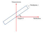
I was wondering what is the best way to set up a HFSS simulation in order to model the transmission and reflection of a germanium mirror at some arbitrary angle. Below is a simple drawing of that I am trying to accomplish

I had a though of how to solve it mathematically, but I want to run a simulation to confirm my thoughts. I treated the problem as a loaded transmission line. The slab of Ge is the transmission line whose length is determined by the angle and thickness. Since this is for an optical setup, the source and load impedance are 377Ω. That could be completely wrong which is why I wanted to run a simulation and ask you all.
My question to the crowd is, what would be the best way to set up such a simulation, in my case for HFSS. My initial thought was to model a small section of the problem as small TEM waveguides with a wave port to excite a linearly polarized plane wave. I attached a picture, not from HFSS, to give an idea.


I envision a 4 port simulation. The left picture shows the square TEM waveguides with the slab of dielectric at a 45 degree angle loading parts the waveguides. The right picture shows the ports and boundary conditions. I represented yellow as e-walls and blue as h-walls. I am not 100% sure those bounty conditions are correct in representing the real problem, but I think so?? The size of the waveguide will be determined by the frequency, λ/2. The white line just shows the polarization to make sure i have TE-mode incidence along the dielectric boundary. I will create the simulation later today but I wanted to get you'll opinion on the matter.
Thanks in advance,
Sam
I was wondering what is the best way to set up a HFSS simulation in order to model the transmission and reflection of a germanium mirror at some arbitrary angle. Below is a simple drawing of that I am trying to accomplish

I had a though of how to solve it mathematically, but I want to run a simulation to confirm my thoughts. I treated the problem as a loaded transmission line. The slab of Ge is the transmission line whose length is determined by the angle and thickness. Since this is for an optical setup, the source and load impedance are 377Ω. That could be completely wrong which is why I wanted to run a simulation and ask you all.
My question to the crowd is, what would be the best way to set up such a simulation, in my case for HFSS. My initial thought was to model a small section of the problem as small TEM waveguides with a wave port to excite a linearly polarized plane wave. I attached a picture, not from HFSS, to give an idea.


I envision a 4 port simulation. The left picture shows the square TEM waveguides with the slab of dielectric at a 45 degree angle loading parts the waveguides. The right picture shows the ports and boundary conditions. I represented yellow as e-walls and blue as h-walls. I am not 100% sure those bounty conditions are correct in representing the real problem, but I think so?? The size of the waveguide will be determined by the frequency, λ/2. The white line just shows the polarization to make sure i have TE-mode incidence along the dielectric boundary. I will create the simulation later today but I wanted to get you'll opinion on the matter.
Thanks in advance,
Sam