Continue to Site

Welcome to EDAboard.com

Welcome to our site! EDAboard.com is an international Electronics Discussion Forum focused on EDA software, circuits, schematics, books, theory, papers, asic, pld, 8051, DSP, Network, RF, Analog Design, PCB, Service Manuals... and a whole lot more! To participate you need to register. Registration is free. Click here to register now.

Input Matching Network question

Status
Not open for further replies.

pYrana13

Junior Member level 1
Joined
Nov 29, 2009
Messages
16
Helped
0
Reputation
0
Reaction score
0
Trophy points
1,281
Activity points
1,407
Hi all,

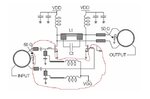
I came across this RF class-D power amplifier design and want to know, what type of input matching has been used here? I cant really understand the input matching schematic below(shown in the red region). Is it only for matching purpose or is there any other purpose? Could someone please explain it to me?

Thanks a lot.
 

Attachments

  • cmc.JPG
    cmc.JPG
    47.3 KB · Views: 62

Is not a particular type of impedance match. The series gate inductors are used to resonate the internal Cgs of the FETs. Also there are two identical high-impedance bias networks (for Vgg), most probably using quarterwave TL, series chokes, and decoupling caps.
The blocking caps (in series with gates) can be used for narrowband matching together with the afferent series TL, and the shunt TL (which goes to Vgg). But this statement is not mandatory in a wideband matching.
 

Matching to switchmode amp gates isn't an exact science, in my experience. For my class D amps I use an inductor in series with the gate, and then a shunt capacitor. That circuit could work too though.
 

Status
Not open for further replies.

Part and Inventory Search

Welcome to EDABoard.com

Sponsor

Back
Top