Continue to Site

Welcome to EDAboard.com

Welcome to our site! EDAboard.com is an international Electronics Discussion Forum focused on EDA software, circuits, schematics, books, theory, papers, asic, pld, 8051, DSP, Network, RF, Analog Design, PCB, Service Manuals... and a whole lot more! To participate you need to register. Registration is free. Click here to register now.

Increasing the current handling capability of linear voltage regulators

Status
Not open for further replies.

khatus

Member level 3
Joined
Oct 7, 2017
Messages
56
Helped
1
Reputation
2
Reaction score
0
Trophy points
6
Activity points
441
Hello guys, I want to calculate the value of resistor R1 in the figure. But while doing the calculation I face the following problem
First, see the pictures below,
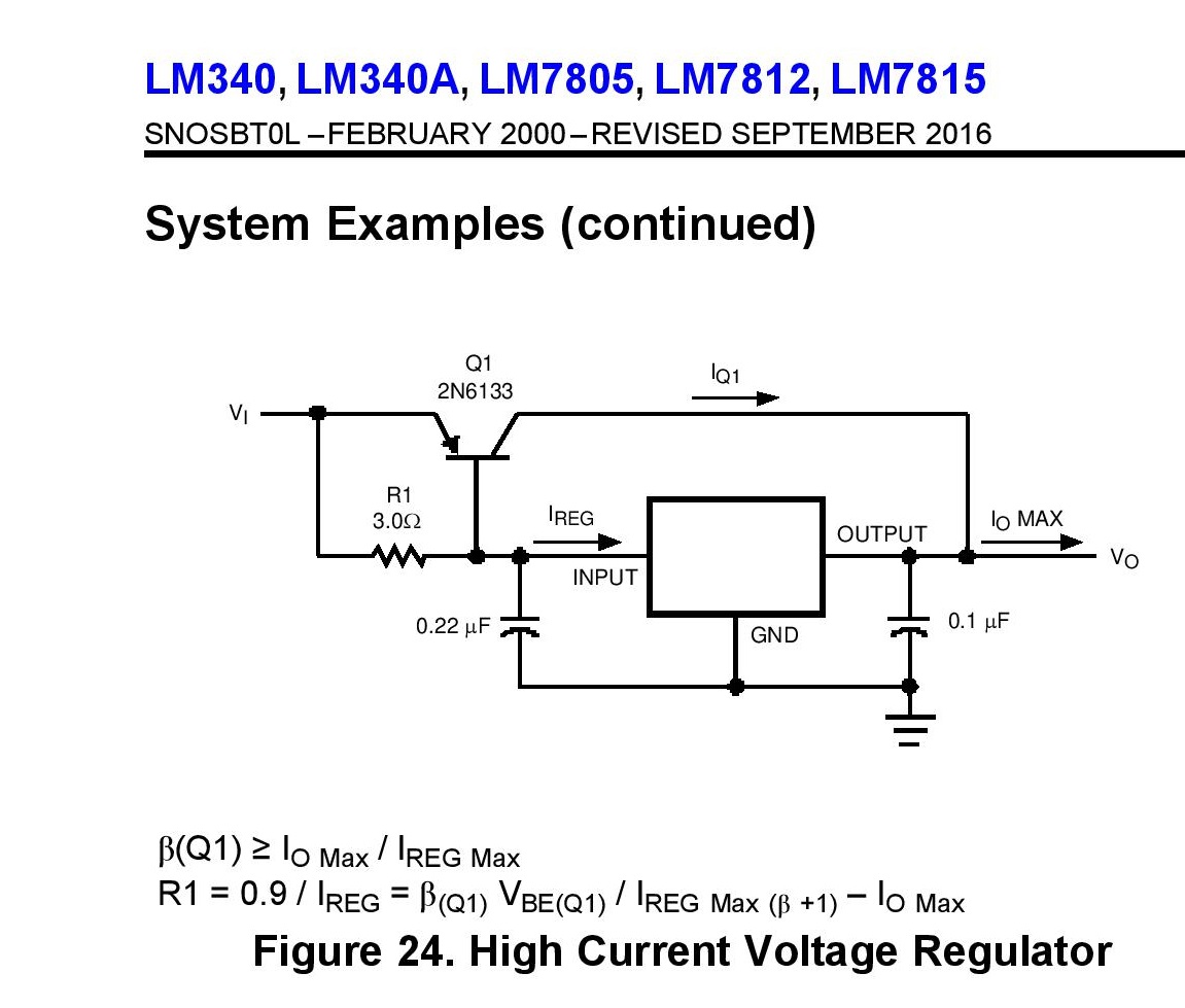
lm340-page-016.jpg


In my calculation, VBE =0.7 = I1* R1 to turn the transistor on. But here, but Here I1 = IREG was taken, so that
R1 * IREG = 0.7 volts.
I did not understand this part, In my calculation,
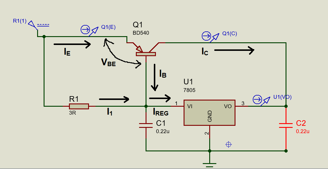
Input-current_question.PNG


At the junction,

I1+IB = IREG

IREG - IB = I1

Now the Beta of the transistor is known and From the output current I can calculate IC and I can find IB from IC.
a) So I1 and IREG are not the same. So how did equal this two here?
b) Where can I find the maximum value of IREG?
c) To calculate the output current I need at least two quantities from ( I1, IB, IREG). How i can determine these two quantities
 
Last edited:

In both cases Ireg = Ibase_pnp + Ir1

But for a reasonable transistor, at max load on output, the base current
can be neglected due to its beta. So to a first order approximation to
have a max load, a % thru PNP, a % thru reg. So compute the R for its
percentage of current that will go thru reg, and Vbeon as the V across
it to have the PNP do its fair share.

Do a spice sim once you do this computation and sweep the load to see
that sharing is met. Sweep over T so you can see the worst case.


Regards, Dana.
 

Hi,

To decide Ireg, apart from Vreg Imax. and PDmax. in datasheet, you can choose! Maybe you want the bypass transistor to turn on at 100mA or at 1A, from there just calculate the resistor needed for the required voltage drop which will fully turn on the PNP at that defined current. Unless you actually know the beta value precisely or need to be certain, I'd just choose 10 or 50 or 100 and not overly worry about that figure.

I find this a useful but 'messy' circuit - the transition from I through Vreg to I through PNP is gradual and some current still flows through Vreg anyway, and the resistor has to dissipate all the current until PNP is fully on, and it's in series with Vreg input, but still, still good.

PS - check PNP Veb details (specs and confusing graphs) in datasheet well, and maybe extrapolate from their test set-up values where your application's values fit into those parameters closest, and you might actually want to aim for -0.9Veb or even -1.2Veb to ensure it is fully on when you need it to be on (and extra points for factoring in temperature range of use and its effect on '0.7' Veb).
 

There is no exact right or wrong value, you choose how much current flows through the regulator before the transistor conducts. I usually pick about half the anticipated load current as the turn on point, so if you follow my recommendation, use R=0.7/(load current / 2) as the value. The advantage of this circuit is the overload and over-temperature shutdown of the regulator also shuts down the transistor current. If possible mount the regulator and transistor on the same heat sink so excess dissipation in either one will shut them both down at the same time.

Brian.
 

A rough sim of the sharing, sweeping load....

1665357240377.png


Regards, Dana.
--- Updated ---

You have to juggle the R to get the worst case power thru reg in spec.
Eg. the junction T limits, and associated thermal R. Here is a case that
looks better for U1 Pdiss :

1665357983852.png


Regards, Dana.
 
Last edited:

Hi,

The BD540 is a power transistor so we should expect it to have a low beta. In fact, its data sheet values confirms this. so, the base current should not be neglected.

I'd recommend you use the minimum value of beta as given in the datasheet.
Iout(worst case) = Ib*(beta + 1) + IR1
So if we let Ib to be one-tenth of IR1, we have: Iout(worst case) = 0.1*IR1*(beta + 1) + IR1
So that Iout(worst case) = IR1*(1.1 + 0.1*beta)
Therefore,
IR1 = Iout(worst case) / (1.1 + 0.1*beta)
R1 = Vbe/(IR1)
 

If Ib1 = Ic1`/10 then the transistor is ~ in saturation, eg. very little Vce change
with Ib change, no longer able to "regulate", act as a variable R.....

1665392268791.png


Regards, Dana.
 

Hi,

basically with the given circuit you have two operation modes:
mode1) low current: all the load current is delivered by the regulator (V_R1 < V_BE)
mode2) high current: a part of the load current is provided by regulator but now the BJT provides additional current.

The value of R1 decides at which load current there is a move from mode1 to mode2.

***
I see no additional "waste of power". No additional "heat". Since to current through R1 also goes to the load ...
(as long as the input voltage isn´t very close to the minimum operation voltage of the regulator)

Klaus
 

Small change in efficiency as load is swept from 10 to 1 ohms, Q1 non linearities.....maybe.


1665396777414.png


Regards, Dana.
 

I want to clarify one thing, the input current of voltage regulator and the output current of voltage regulator will be the same for a particular load?

input_and_outpyt_current.PNG
 

If you take a look at Figure 7.2: Functional Block Diagram of this datasheet https://www.ti.com/lit/ds/symlink/lm7800.pdf, for example, you'd see that not all the input current pass through the pass transistor. So the output current is less than the input current, just like Dana has mentioned. However, the question that remains whether how much is the difference.
--- Updated ---

Considering the value of the quiescent current as given in the datasheet suggests that the difference is negligible.
 

If you want lin regs with higher current...put them in pllel with load share circuitry...as in the attached LTspice and pdf.

Modus operandi:
As you can see it operates just like the UC3902…..all that’s needed is to put out a “share” bus (differential) which is just simply the highest current sense voltage of all of the paralleled stages. Then an error amp is fed this, and also fed the actual stage’s own current sense signal (with 100mV added to stop chattering)……and that then gives you all the paralleled stages sharing current nicely. The stages are simply throttled/accelerated in current output by pulling current through a resistor in the vout divider. The error amp does this via a common base and reference.

The signal voltages are near zero volts so all opamps need pos/gnd/neg supply.

The simulation does take ages to run. (any tips on speeding it appreciated). The sharing error amp is way too fast compensated, but had to be or else the sim takes till xmas.

UC3902 datasheet:
https://www.ti.com/product/UC3902
 

Attachments

  • Linreg with Load share_works x3 diffbus__Remotesenres_diffrentGNDs.zip
    10.2 KB · Views: 102
  • Lin regs in pllel_221010.pdf
    226.8 KB · Views: 129

Small change in efficiency as load is swept from 10 to 1 ohms, Q1 non linearities.....maybe.


View attachment 178997


Regards, Dana.
This is very interesting! I would have expected that efficiency would drop with decreasing R or increasing output current.

But then I note that you have not defined the efficiency. for this circuit, I would "dumbly" define efficiency as the ratio of output power to input power.

I would also imagine that higher the input voltage, the lower is the efficiency (the circuit has to drop a larger voltage that will cause higher inefficiency).

Certainly I am missing something. Most likely "what is efficiency, in this case?"
Efficiency was defined as (Pload/Pin) x 100.

Raising Vin to 24V the efficiency drops -

1665483582375.png


Regards, Dana.
 

Hi,

So it is the efficiency in %.

I don´t understand: where does the "-" come from in your charts?

Klaus
It comes from some logs. I mean logarithms. (it was introduced as a torture device for young students).

Obviously efficiency cannot be greater than one. And it must be greater than zero. Log of a number 0<x<1 is a negative number.

Some wise men decided to make numbers large by multiplying with 10. But for power measurements, it is usually multiplied by 20. But it is better with an example.

-20.800 dB of efficiency is be 10^(-20.800/20)=10^(-1.04)=1/10^(1.04)=1/10.96=0.091 (efficiency is about 9%)

Forgive me if I am wrong. But I doubt that the curve says the efficiency is around 20%
 

Status
Not open for further replies.

Part and Inventory Search

Welcome to EDABoard.com

Sponsor

Back
Top