Continue to Site

Welcome to EDAboard.com

Welcome to our site! EDAboard.com is an international Electronics Discussion Forum focused on EDA software, circuits, schematics, books, theory, papers, asic, pld, 8051, DSP, Network, RF, Analog Design, PCB, Service Manuals... and a whole lot more! To participate you need to register. Registration is free. Click here to register now.

Incorrect sampling in a tapped delay line

Phrancees69

Newbie level 6
Joined
Feb 16, 2022
Messages
12
Helped
0
Reputation
0
Reaction score
0
Trophy points
1
Activity points
117
Hi,
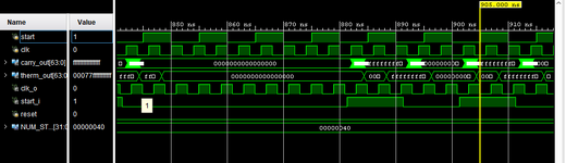
I am working on a TDL TDC using carry4 elements as my delay line. I currently have a delay chain of length 64. The propagation delay of the each carry4 is 118 ps. I have tried to sample the TDL output using D flipflops clocked by 10 ns. The output of the DFFs do not sample correctly (no update on clock's rising edge). I am new to FPGAs and digital designs. I have tried using an LSFR and a wave union tecehnique to supply the start signal but results are no different. Kindly assist. thank you
 

Attachments

  • tdl.png
    tdl.png
    18 KB · Views: 67
I would not trust a logic simulator to do this work. There
is too much "simplification". A flip-flop sampling delay has
significant variation as your setup time approaches the
metastable point and somewhere, the captured states will
be unreliable before turning reliable again.

You might (if you get any capture, and why wouldn't you?)
apply a secondary layer of logic to determine the "most
likely center" of the "wavefront" as it slides past the clock
edge. There should be unbroken stretches of "0", a few
bits' worth of "flicker" and then unbroken stretch of "1",
right? If you can "bound the flicker" and "pick the center
of that", maybe you can assign a center "more reliably"
than the raw registered bits.

I did something like this on a burst mode clock recovery
unit design, once.

You could also (as I did there) use a scheme where you
"clock the clock, with the data" - let each stage of the delay
loop clock in the same 10ns master clock (sets the frame?)
which you'd presumably upscale to get bit-count in time
domain; the 'flops will now capture sequentially and the
code-transition in that field "marks the spot". Might work
cleaner (or not).

I'll note that to make my thing work, I had to hand-design
the FFs and use complementary bare-clocking to cut the
setup time (front latch) and raw delay (back latch) and
even cheat by using low-VT "RF only" devices in the FF
clock legs. That's SPICE w/ full parasitics design. Not a
prayer of reasonableness from a logic simulator (what
would I do with a pile of timing violations? The cell library
the company had, couldn't even self-toggle (D=Q!) over
300MHz and I was on the hook for 400MHz (and a wee
bit of 800) with feedback logic between register stages.
Now imagine 10kGates worth of this done by hand, and
at-speed functional verification in Spectre being the only
available option. 3 years of my life that I ain't getting back.
Thanks for your explanation. The design is implemented in vivado using verilog. I'll try to clock the FFs using the output from each stage of the delay line as you suggested. Keeping fingers crossed. Thanks a lot
 
Last edited:

LaTeX Commands Quick-Menu:

Part and Inventory Search

Welcome to EDABoard.com

Sponsor

Back
Top