jktstance
Newbie level 5
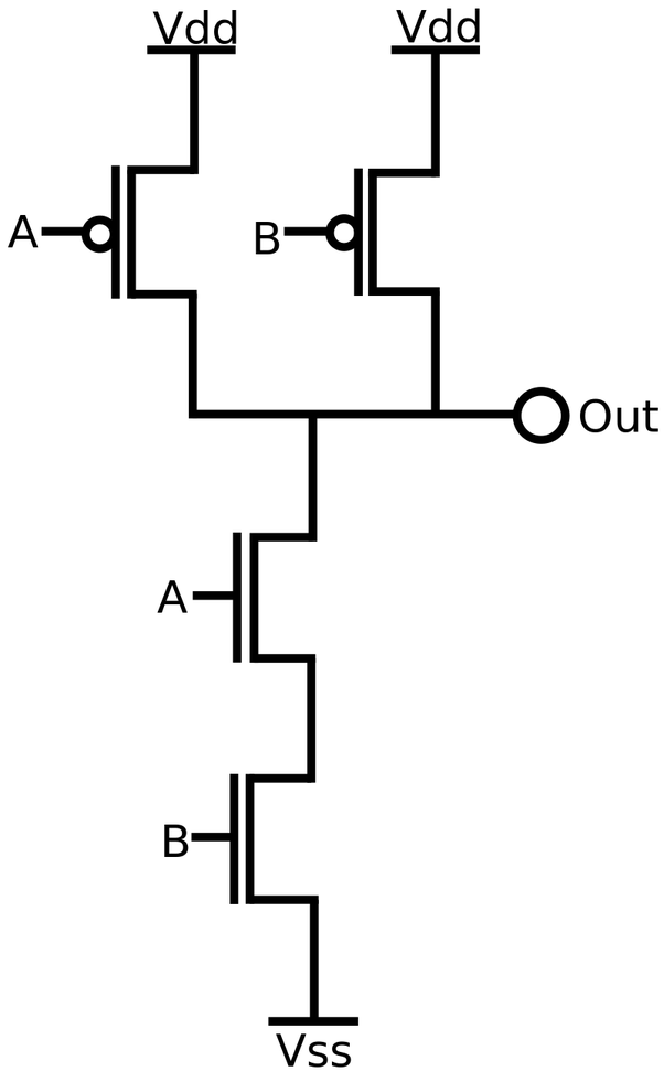
On the image below, if Vout is initially Vdd and A and B are 0, will the gate delay and slew be less if A switches to 1 before B, or vice versa?
I believe the answer is B before A, because if A turns on before B, then the source of A will be pulled up to Vdd, and then pulled down when B opens up. However, I can't really convince myself of that, because why does it matter if Vds of the bottom transistor is Vdd? It will still have to drain 5V. If B turns on first, then the drain of the top nmos will be pulled down to 0, so the top nmos will still have to drain 5V. What am I missing here?

This was an interview question I somehow got right, but I still can't convince myself. I believe the interviewer was assuming the A or B transistor will be fully switched on or off before the other one is enabled, in which case my above question still stands.
If they are not fully on and drain all of Vds before the next one does, then I can imagine B before A being correct because if B conducts first, it is pulling the source of A down, and then when A conducts after it will pull down Vout. If A conducts first, then the drain of B will be pulled up towards Vdd, and then down when B turns on after.
I believe the answer is B before A, because if A turns on before B, then the source of A will be pulled up to Vdd, and then pulled down when B opens up. However, I can't really convince myself of that, because why does it matter if Vds of the bottom transistor is Vdd? It will still have to drain 5V. If B turns on first, then the drain of the top nmos will be pulled down to 0, so the top nmos will still have to drain 5V. What am I missing here?
--- Updated ---
This was an interview question I somehow got right, but I still can't convince myself. I believe the interviewer was assuming the A or B transistor will be fully switched on or off before the other one is enabled, in which case my above question still stands.
If they are not fully on and drain all of Vds before the next one does, then I can imagine B before A being correct because if B conducts first, it is pulling the source of A down, and then when A conducts after it will pull down Vout. If A conducts first, then the drain of B will be pulled up towards Vdd, and then down when B turns on after.
Last edited: