Continue to Site

Welcome to EDAboard.com

Welcome to our site! EDAboard.com is an international Electronics Discussion Forum focused on EDA software, circuits, schematics, books, theory, papers, asic, pld, 8051, DSP, Network, RF, Analog Design, PCB, Service Manuals... and a whole lot more! To participate you need to register. Registration is free. Click here to register now.

Implementing FPU on FPGA using Verilog

Status
Not open for further replies.

psurya1994

Member level 5
Member level 5
Joined
Jun 29, 2012
Messages
86
Helped
3
Reputation
6
Reaction score
3
Trophy points
1,288
Visit site
Activity points
1,807
Is it possible to implement a Floating Point Unit (FPU) (Single Precision IEEE 754 format) on an FPGA which can do all addition, subtraction, multiplication and division? If yes, which algorithms would be good for multiplication and division?

I'm using Xilinx IDE.
 

Yes it is possible. It seems you have multiple options ...
-> Take a look here: https://opencores.org/projects
You will find multiple FPU designs and also dedicated FP arithmetic blocks that all support IEEE754.
-> Use the Xilinx CORE Generator (which is part of the ISE install) to generate functions for you under Math Functions->Floating Point category.
(but this will not give you insight into the source HDL code or algorithms)
 
Thanks! That helped!

I'm looking to publish a paper after implementing this on an FPGA, after suggestions/comments on that?
 

Not knowing what the actual goal is of your project, I'm not sure what to comment on about a paper.
What are you trying to do that has not been done and documented before?
Or is it intended to be of a tutorial nature? (for IEEE 754 concepts, or for FPGA implementation concepts, or for interfacing the FPU as a co-processor to e.g. a CPU?)

You might want to check out Xilinx's own Xcell tech-journal for examples (**broken link removed**), but can those sometimes tend to be of a marketing nature, but not always.

There are also a number of sites out there where people write DIY articles, but again not sure if you are seeking out more of a professionally published venue.

Of course there is also the EETimes/UBM Programmable Logic DesignLine forum/email/blog arena (https://www.eetimes.com/programmable-logic-designline.asp).
You might want to send an email to Max Maxfield who organizes and edits all of that that and get his opinion.

Good luck!
 
My professor at college told me that he will make sure we publish a paper, if we implement a FPU with addition, subtraction, multiplication and division. Everything I'm doing has already been implemented before.

For a typical FPU, how many clocks does it take for various operations? Is it one clock or more?
 

The pipeling length depends on the function, and the desired clock speed. For faster clocks, you need more pipeline. I think typical rates for a decent FMax (about 300 MHz) are about 15 clocks for addition/subtraction, 30 for multiply and 50+ for divide and square root.
 
Thanks for the reply.

Why do we need so many clocks? Why can't we implement it in three clocks for addition?
1. Compare and Shift
2. Add mantissa
3. Normalize output
 

In fact you could perform an addition in *one* cycle using only combinatorial logic, but the propagation delay would require a low frequency for each new operation, and might not be usable for most S/W applications.
Note that the configurable Xilinx CORE Generator IEEE 754 function will let you set latency to 0 for certain operations.
But the OpenCores FPU was instead designed for a specific latency, probably because they felt it was a safe tradeoff to guarantee 100MHz with the Altera Cyclone FPGA that they had available to them at that time (and to make it configurable would have been a lot more work).

There are a couple of tradeoffs that are inter-related with all of this.

One is how pipelining affects latency (# of cycles to get a result through the operation), but does not affect throughput (# of cycles per start of each new operation).
In other words, with pipelining, you can have multiple operations in each pipeline stage flowing together through the overall FPU.

In contrast, throughput will get lowered if you implement an operation sequentially instead of in parallel.
Sequential means you are re-using the same logic resources for different cycles, to save area at the expense of waiting added cycles before a new operation can start.
(note that the OpenCores FPU uses this tradeoff approach, but only for division)

Anyway, I do not want to risk further confusion here.
I think you will begin to become more comfortable with these tradeoff concepts more as you read more, and also as you actually try to implement the design through the FPGA toolset.
Perhaps the Xilinx CORE Generator is good to begin seeing cause & effect with (frequency vs latency), since it supports a configurable number of latency cycles.
(the OpenCores FPU is instead fixed at what they designed it with)
There are probably a lot of decent papers and college course presentations on the web that do a better job of explaining all of this.
 
Thanks Jrwebsterco. Can you please provide me with the resources to learn more about the tradeoffs you mentioned.

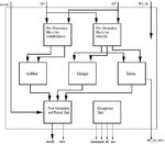
I'm planning to follow this block diagram, where I will implement each of the block take different number of clock cycles. Is it necessary to introduce buffers between each of them?
block.jpg
 

I'm afraid don't have the time to go and chase down references you seek - I do not have any already on hand and you can easily search for them yourself.

I think that you are getting into usage and flow and handshaking details, which is something you would need to think through as part of your project.
If you read through the docs (PDFs) for the different OpenCores FPU projects, and also for the Xilinx cores, you will notice the following trends:
-> The Usselmann FPU will not provide a "ready" or "done" output flag, but instead accepts new data on every cycle and has the exact same number of cycles of latency (4 cycles) per *any* operation (but it is also not able to run at a very high frequency since it is only a four-deep pipeline even for e.g. a divide).
-> The Jidan FPU instead outputs a "ready" signal, which must be used to know when a new data can be fed into it, but this also allows a different number of cycles for different operations.
-> The Xilinx core does not support multiple operations in the same core (you would need to combine a few of these together with added logic to create a true FPU).

I think you can easily gather and understand knowledge for yourself.
There are certainly more papers out there about how to approach the pipelining and balancing and data-flow issues with an FPU design.
For example, I just now searched for "fpu design pdf" and quickly found the following: ftp://reports.stanford.edu/pub/cstr/reports/csl/tr/96/711/CSL-TR-96-711.pdf
Maybe you could start reading through this and also consider some of the references listed in the bibliography?
Good luck with your project ...
 
Status
Not open for further replies.

Similar threads

Part and Inventory Search

Welcome to EDABoard.com

Sponsor

Back
Top