Dummyeng
Member level 4
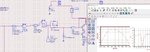
HI
I want to design an Impedance matching line for transistor and in loadpull design i found out that 50 should be 0.3+j*1.8
i try to do it with smith chart in ads and i found out it is very hard
first i put q=2 circle and i want to do it in this circle but it is impossible
my frequency is 0.9 to 1.3 Ghz
should i first consider bode-fanno law?
or i can try harder
is there any approach that i can use that?