Continue to Site

Welcome to EDAboard.com

Welcome to our site! EDAboard.com is an international Electronics Discussion Forum focused on EDA software, circuits, schematics, books, theory, papers, asic, pld, 8051, DSP, Network, RF, Analog Design, PCB, Service Manuals... and a whole lot more! To participate you need to register. Registration is free. Click here to register now.

Impedance controlled trace in between GND and POWER planes?

Status
Not open for further replies.

popoyboys

Advanced Member level 4
Joined
Feb 20, 2007
Messages
110
Helped
4
Reputation
8
Reaction score
2
Trophy points
1,298
Location
from the deepest roots of KAMOTE land
Activity points
1,967
I'd like to know what are the implications and effects of having an impedance controlled routes stacked in between a GND and POWER plane layers.
I'd like to hear your comments/feedback/suggestions.

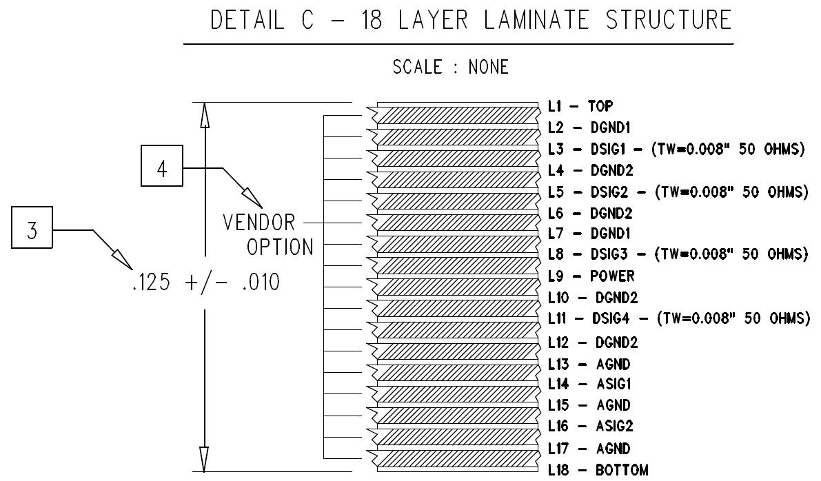
I have attached my stackup here and I am referring to Layers 7, 8, 9.


Splits in power plane layers can cause signal integrity issues if the signals couple to these layers. There has been quite a long previous post on this. I'll try and find it later.
Interesting to see analogue and digital grounds, especialy in that format (on top of each other), I think one ground is better, with demarked areas of analogue and digital circuitry, with your stack any through vias will couple digital noise down to the analogue planes, or you use a very complesx system of blind and burried vias.
 

This is the configuration for stripline, having the impedance controlled trace stacked in between reference plane. We have to pay duly notice especially for the case in between GND and PWR plane, knowing that the EM field of the trace spread both above and bottom to the plane. Any traces that unintentionally crossed the split of PWR plane may cause impedance discontinuity. While it is not feasible by having too many ground planes just for the sake of stripline routing, causing increased stackup layers.

This is one of the problem that I did not know how to solve for the case of BGA package, having bunch of traces routed away from the BGA passing through splits of planes using stripline (we knew that several voltages are used for BGA).
 

The usual thing to do is to make sure that you have decoupling capacitors (10nF) close to the start and the end of the signal trace. This enables the return current to enter the power plane and follow the signal track. The return current in the GND plane would go anyway, ensured by the GND pins on the TX and the RX chips. If you have adequate return paths provided in both below/above planes (right under/below the signal track), then the impedance calculation (for example using polar SI8000 or TNT-MMTL) would leat to accurate results.

Another thing is in most of my designs I don't have power planes, I use mixed signal/power layers and lots of GND planes. If you have lots of gigabit signals, then I would recommend this approach to you. I have power planes on 14+ layer PCBs, between the out-most GND plane and the outer (top or bottom) layer. Also, the top/bottom layers don't have any or many impedance controlled tracks, only fanout. Usually short fanout tracks are not impedance controlled anyway.
 

Or you can have specific layers for high speed signals that are true stripline (between two grounds) and run other non-critical slower signals on other layers, where the signal coupling isn't as critical.
 

I think the power plane better with single pour power beside the trace,the power with a power decouple, in theroy, we could treat the power pour as a 'GND'.
 

A single pour power will act quite happily as a return path, the trouble is with todays designs having enough layers to do this, or to keep layer count down have multiple pours on the power layers.
PCB design is a combination of balancing SI and EMC, cost, requirements and about a million other things, at the end of the day we get the boards to work, despite all the fun on the way.
 

Another thing is in most of my designs I don't have power planes, I use mixed signal/power layers and lots of GND planes. If you have lots of gigabit signals, then I would recommend this approach to you. I have power planes on 14+ layer PCBs, between the out-most GND plane and the outer (top or bottom) layer. Also, the top/bottom layers don't have any or many impedance controlled tracks, only fanout. Usually short fanout tracks are not impedance controlled anyway.

Buenos, how do you make sure PI in this case by having signals mixed with powers? Besides, shouldn't we control the impedance for fanout also during high speed condition?

Or you can have specific layers for high speed signals that are true stripline (between two grounds) and run other non-critical slower signals on other layers, where the signal coupling isn't as critical.
Marce, I have stackup constraint that does not allow me to have true stripline, between ground and mixed power planes, how should I route my critical signals after fanout?
 

its better to control impedance on fanout, but usually its not possible. try to make short dog-bone fanout insteaddd of long-reaching fanout, then you dont need impedance control on it.

signals mixed with power on same layer? signal tracks and copper pours (power delivery) don't effect each other, since they are on the same layer, they dont overlap. In this stackup: top-GND-sig1-GND-sig2-sig3-GND-sig4-GND-bottom sig2/3 has no sensitive high-speed tracks, so even an overlap would not effect the signals on them.
 

Status
Not open for further replies.

Part and Inventory Search

Welcome to EDABoard.com

Sponsor

Back
Top