Continue to Site

Welcome to EDAboard.com

Welcome to our site! EDAboard.com is an international Electronics Discussion Forum focused on EDA software, circuits, schematics, books, theory, papers, asic, pld, 8051, DSP, Network, RF, Analog Design, PCB, Service Manuals... and a whole lot more! To participate you need to register. Registration is free. Click here to register now.

IGBT switching loss control

Status
Not open for further replies.

xeratule

Member level 4
Joined
Apr 4, 2009
Messages
69
Helped
1
Reputation
2
Reaction score
1
Trophy points
1,288
Location
Istanbul / TURKIYE
Activity points
1,975
Hi all,

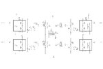
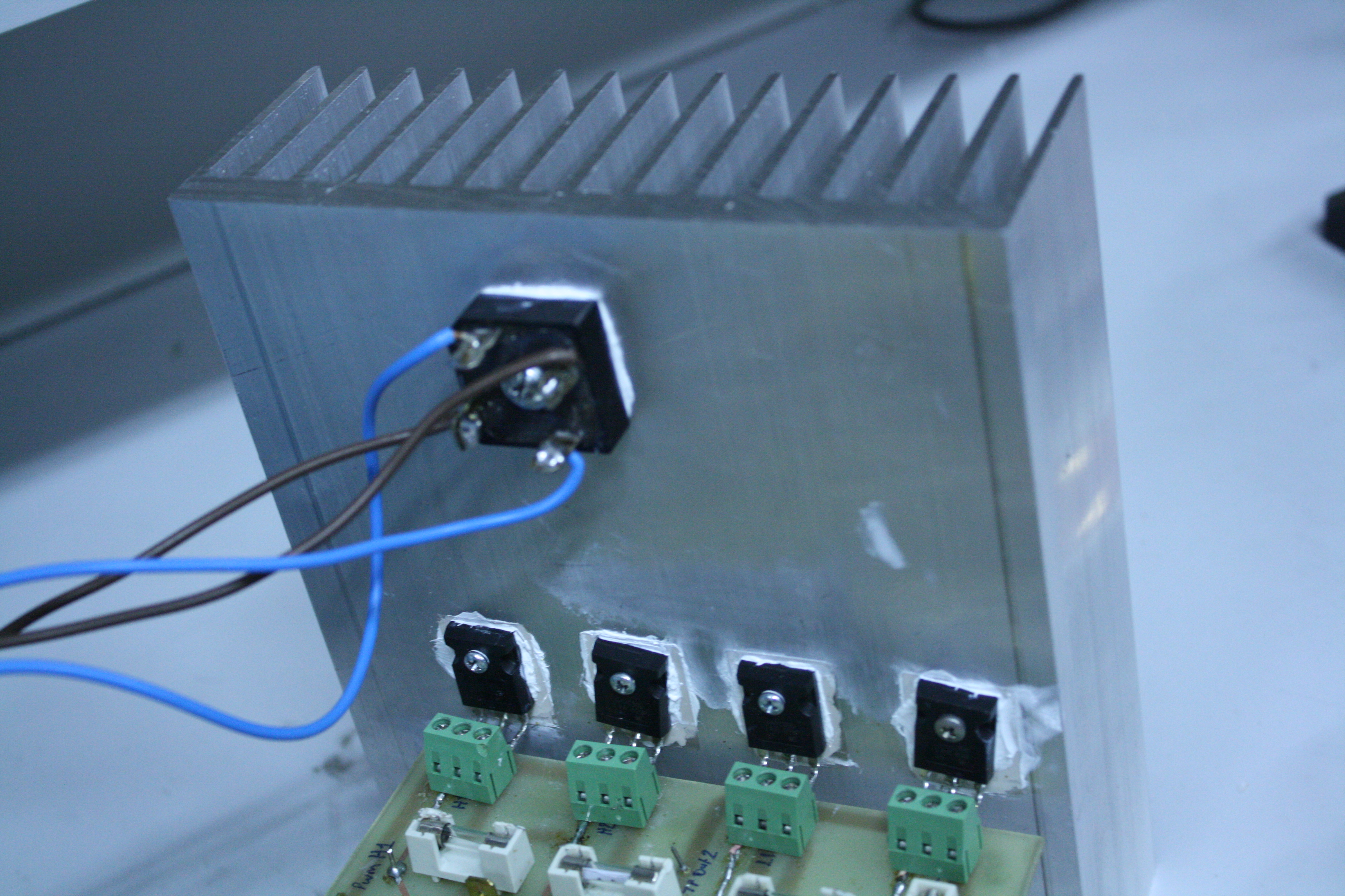
I am using high power (600V,12A @ 100°C) ultrafast IGBT's in a full bridge circuit configuration. The gates are driven with push pull PWM.

The IGBT's get overheated and fail when draining only 4.5A collector current. (Although IGBT's are bounded to a passive aluminium cooler with fan support).
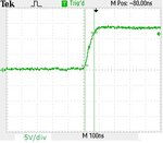
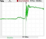
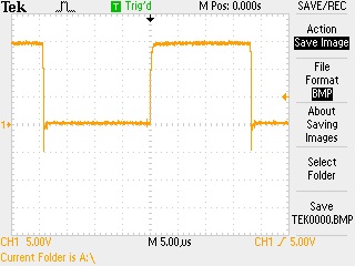
I know if PWM signal is not sharp at edges that will cause switching loss. The gate PWM signals seems sharp enough when I don't supply the collector of the IGBT's. When I supply with 220V (Vcc) and IGBT's start to drain current the gate signals get noisy. Please see the attached gate rising edge signal measurements with and without Vcc supply voltage. Do you think that causes the big portion of the temperature rise? What causes this ripples and how can I get rid of them?
Why else do they overheat?

Would like to hear from you soon. Thanks in advance.

Erhan
 

Attachments

  • clear_60ns.jpg
    clear_60ns.jpg
    23.1 KB · Views: 127
  • noisy_60ns.jpg
    noisy_60ns.jpg
    24.1 KB · Views: 163

If IGBT's are not driven correctly power loses can be high enough to destroy the device... Have you checked that high side and low side IGBTs are not turned on at the same time, changing the deadtime would avoid this situation. Is the figure you are sending from high or low side switch?
Provably the gate driver circuit you does not perform correctly... Is it isolated? having the circuit schematic would be of great help!

Ernest
 

Would be helpful if you post a schematic on this.

1. Do note that for any power electronic devices, switching loss is not the only cause of power loss and usually very small percentage. I believe the major contributor of heat comes from the conduction loss. Maybe you can measure and check the input current and output current of the IGBT again.

2. Noisy is the inherent nature of PWM circuits (due to switching noise) and Bipolar devices (due to electron-hole pair recombination). You can maybe able to have less noise that by using Power MOSFETs. Add filter caps and zener diodes to reduce the ripple.
 

Yeah that gate waveform looks pretty bad. You might actually be seeing some RF oscillation as the device transitions from cutoff to saturation. May also be diode reverse recovery as well. Try adjusting the dead time of the bridge. Also the gate voltage seems to sag a bit after the initial rise... that's no good.

What's your switching frequency by the way?
 

My first question is, if the waveform is showing the actual gate voltage and not just a measurement artefact due to unsuitable probing. The high frequency oscillation indicates that something bad is going on in any case. But the problem can't be analyzed by only looking at the gate waveform. It's important to know, that the bus voltage has sufficient low inductance bypass capacitors and is wired appropiately. Also, you should clarify that the opposite bridge transistor is previously switched off and kept in this state during turn-on of the transistor of interest.
 

Have you checked that high side and low side IGBTs are not turned on at the same time, changing the deadtime would avoid this situation. Is the figure you are sending from high or low side switch?
Provably the gate driver circuit you does not perform correctly... Is it isolated?

The high side and low side IGBT's have safe dead time protection. All IGBT gate responses in the circuit are similar. Isolation is covered by optocouplers pls see the attached circuit.

Would be helpful if you post a schematic on this.

1. ...I believe the major contributor of heat comes from the conduction loss...
.

Could we do anything to decrease conduction loss? From the datasheet figure 1: IGBT's can operate safely at 10A collector current with 30khz %50 duty cycled pwm. I don't think that's the issue.

2. ... Add filter caps and zener diodes to reduce the ripple.

Already have TVS diodes. Wouldn't filter caps increase gate charge time and that's why increase switching loss? Please see the schematic.

What's your switching frequency by the way?

The pwm signals are @ 25 khz. I think I have pretty important issues at 15V supply rail. Please see following explanations.

It's important to know, that the bus voltage has sufficient low inductance bypass capacitors and is wired appropiately. Also, you should clarify that the opposite bridge transistor is previously switched off and kept in this state during turn-on of the transistor of interest.

There is neither probing, nor same time switching on failure (proper dead time is arranged). But, yes I noticed important switching noise at 15V supply rail. Maybe that causes the optocoupler to switch off for a short time. This noise should be the ground bounce caused by switching IGBTs. Please see the figures below. They are low side IGBT gate rise and fall times with different view. Clear signals are (named as closed) when Vcc is not applied to IGBT's. You can see dead time clearly.
View attachment rise_closed.BMP
View attachment rise_open.BMP
View attachment fall_closed.BMP
View attachment fall_open.BMP

How can I neglect ground bounce that effects 15V supply rail?
 

Attachments

  • schm.jpg
    schm.jpg
    139.1 KB · Views: 199

Low ESL and ESR caps have integral that can damper the overshoots & undershoots. As seen in your waveform, the shoots look oscillating for while when your IGBT switches.
You need caps for sure, but you can use them later as you want to find the ROOT cause of the problem.

OK, since you have TSV, I believe you have adequate protection.

I saw you mentioned overheating in your IGBT. If you don't have this problem, then conduction loss is very negligible.
Just FYI if you still encounter overheating problem, you may have to check if your IGBT is working within Safe Operating Area (SOA).

From your schematic, looks like you are driving a piezo-actuator isolated by a transformer and the driving technique is a H-bridge. Am I right?
If so, I think I see where your problem MAY BE.
Transformer (like inductor, solenoid and relay) is also a coil, then Lenz's Law and back emf applies. The back emf may be the root cause for the oscillation as it NET the current and voltage as your IGBT switches.
This NET voltage and current are seen as overshoots and undershoots, until the back emf is totally weaken by your driving voltage and current.

So far your waveforms are showing NET voltages, so we can put aside the current for later analysis. You may want to improve on providing a back-to-back clamping diode or TVS to the transformer.
 
Last edited:

To understand if there may be a problem with driver supply voltage drops, you should tell about the driver type. Does it have an undervoltage lockout feature? The other explanation would be, that interferences are coupling to the input (LED) side.

I don't expect an transformer EMF problem, but did you test the power stage without the transformer load, e.g. with a resistive load? The load current can be monitored with a small homemade current transformer.

You can also try to decrease the switching speed by increasing the gate resistors for test and check, if the oscillations stop, respectively how they are modified.
 
Capacitors C1 C4 C5 C6 must have more than 100 nF. This will reduce your Vboostrap ripple and improve your driver performance. Note that that you are draining a peak of > 1 A when charging the IGBT gate. This would explain the voltage dips in +15V.
Use 1 uF X7R MLCC caps as close to the driver as possible. Also reduce track lenghts between driver and IGBT if possible. Some gate drivers have undervoltage lockout protection (UVLO) when supply voltage falls below a specified limit. If the voltage dip (due to the charge current) exceeds UVLO voltage the driver would turn off.

I agree with SkyHigh that adding low ESL and low ESR DC bus capacitors would improve the behaviour of the system. These capacitors should also be placed as close as possible to the IGBT bridge. Film capacitors (MKP or MKT) are typical in this applications.
 
  • Like
Reactions: FvM

    FvM

    Points: 2
    Helpful Answer Positive Rating
As the circuit benefits from bootstrap capacitors it won't operate when not using them. Does through hole capacitors have different ESL,ESR values? I would try them later. I increased capacitor values but it doesn't even matter. Ripples are still there.

I don't think back emf is the root of the gate signal integrity. Because when I applied resistive load instead of the transformer, still same issues are seen.

I think IGBT's operate well within the SOA. Actually I don't know the all recommendations but they don't operate above voltage and current limits. Gate charge is fast enough and Vge=15V as typical. From the datasheet they can operate in switch mode safely at 10A, 30khz at %50 duty cycle. IGBT's are 600V tolerant and operating voltage is 220V rms. Still besides having overheating problem, high transients at IGBT Vce's is another problem. Peak voltage is 310V but high transients reaches up to 500V maybe more. Maybe this is the result of back emf huh? And those transients could stress the IGBT's much and results in overheating?

Coupled interferences are neglectibly small. And yes it has UVLO. Please see the attached table.

What can I do with UVLO?
I also tried to increase gate resitors from 10 ohms to 22 then 47 but oscillation still occurs.
 
Last edited:

For the driver side, you can achieve minimum series L and R values with SMD ceramic capcitors. The high voltage bus should be bypassed with low inductance foil capacitors.

As long as you observe irregular (ringing) switching, transient overvoltages and excessive switching losses aren't surprizing. Getting clean switching edges should be therefore the first objective. We previously guessed about UVLO causing the multiple edges. But if I understand the data correctly, the UVLO turn-on delay would prevent fast switching as observed. So I tend to prefer the other explanation for the time being, feedback to the primary side.

I generally believe, that the issue can be identified by thorough measurements and "intelligent" test conditions.
 
Last edited:

xeratule,

1. Is this transformer built to operate in your intended frequency?

2. Is it possible for you to make an electrical model and simulate this? I am thinking you may have to look at the problem from Control Engineering persepctive to tackle oscillations.

3. Did the IGBT datasheet highlight any suggestions or recommendations when used in similar applications like yours?

4. Did you check on the Internet if anyone has used this exact IGBT parts and they may have faced problems like yours? Sometimes it may be component issues and there could be work-around solutions posted online.
 

firstly you need to put turn off diodes (schottky, 40V 1A) across your gate resistors to give a faster turn off of the IGBT's. From the IGBT are you using, 220VDC applied in 10nS across the device will give 2.8V approx on the gate (gate rise when other device turns on) due to the C-g capacitance and the g-e capacitance. I see that that the typical switching losses are 3.5watts per device for 220VDC and 8 amps, 25kHz, the cond losses will be 8 watt ave per device (@ 8 amps) giving 12 watts approx per device, or 48 watt total, assuming you are using a quality insulator with good thermal properties from device tab to h/sink (with good mounting pressure) you will need a a sink that can dissipate 48 watts with a T-rise of only 1 deg C/watt or so - this is a fairly substantial heatsink (or needs a fan) At high temp the storage (or turn off delay) time can get quite large (180nS + 140nS current fall time 320nS total) and lead to shoot through conduction losses - i.e your dead time may be inadequate at high temps. Also with 10 ohms you can turn on an IGBT fairly fast and this may cause the other IGBT in the bridge leg to come on briefly when its Vce is changing rapidly(as mentioned above) - i.e. the pull down turn off of the gate drive may not be good enough and may need a negative bias - some IGBT's are much better than others in this regard (Fairchild very good) - I imagine this is the root cause of your problems and the cause of the noise noted on the turn on gate waveform - and other places - also do you have a picture of your heatsinking? - as it may be too small for your application. Regards, Orson Cart.
 
Last edited:
  • Like
Reactions: FvM

    FvM

    Points: 2
    Helpful Answer Positive Rating
I agree about the shoot-through explanation. But we don't know the output characteristic of the gate driver (the type hasn't been revealed yet). Thus I doubt, that adding schottky diode will help without increasing the gate resistors at he same time.

I was under the assumption, that these small IGBTs can work suitably with simple unipolar gate drivers. If this isn't the case, I wonder if one should better go for bipolar drive as used in high power applications.
 

There is neither probing, nor same time switching on failure (proper dead time is arranged). But, yes I noticed important switching noise at 15V supply rail. Maybe that causes the optocoupler to switch off for a short time. This noise should be the ground bounce caused by switching IGBTs. Please see the figures below. They are low side IGBT gate rise and fall times with different view. Clear signals are (named as closed) when Vcc is not applied to IGBT's. You can see dead time clearly.
View attachment 57287
View attachment 57288
View attachment 57289
View attachment 57290

How can I neglect ground bounce that effects 15V supply rail?
So wait, these are just waveforms of the low side FET gates (Q3 and Q4)? What I'd like to see is the gate waveforms of a single half bridge (Q1 and Q3 or Q2 and Q4). Or, if you don't have an isolated probe, show the gate waveform of a low side gate and its drain voltage. It looks like you may be suffering from capacitive coupling from drain to gate, but it's impossible to tell for sure with those waveforms you posted.
 

So I tend to prefer the other explanation for the time being, feedback to the primary side.

I see the ground bounce also effects the primary side. But I think I should solve the issue at high power ground.

1. Is this transformer built to operate in your intended frequency? .

Yes it's an E core 65x27cm. We adjust and do the winding and choosed litz wire suitable for this frequency and current limits.

2. Is it possible for you to make an electrical model and simulate this? I am thinking you may have to look at the problem from Control Engineering persepctive to tackle oscillations..
I can't simulate transformers with my current program. I also wish I could do layout EMI simulation.


3. Did the IGBT datasheet highlight any suggestions or recommendations when used in similar applications like yours?.
I also contact the manufacturer, they didn't say any restrictions about this purpose of use.


4. Did you check on the Internet if anyone has used this exact IGBT parts and they may have faced problems like yours? Sometimes it may be component issues and there could be work-around solutions posted online.
I am new at power electronics so actually could you suggest me some links about this type argumets.

Dear Orson,
I actually have problems while draining only 4.5A with 220V supply voltage. I think I shouldn't have that much loss at this level. I 'll first solve my basic problems then should think about shoot through problems. I measure the Vce rise and fall times and see no shoot through problem as fixed dead time is quiet adequate. Am I missing something here? And please see the attached heatsink photo. It is used with fan support. Is'nt it enough for 4.5A?

After solwing overheating and transient issues I'll try to solve further issues which will appeat at 10A.

...if you don't have an isolated probe, show the gate waveform of a low side gate and its drain voltage.

I don't have isolated probes. Please see the attached single (high side) IGBT Vge and Vce waveforms.
 

Attachments

  • Vce-Vge - 47ohm.rar
    26.2 KB · Views: 85

I 'll first solve my basic problems then should think about shoot through problems. I measure the Vce rise and fall times and see no shoot through problem as fixed dead time is quiet adequate. Am I missing something here?
The assumption is in fact, that shoot-through is the basic problem, also causing excessive losses. The problem is not about missing dead time but self turn-on of transistors due to Cdg capacitance. The gate waveform would look like the observed ones in this case.
 

From what I understand I need to connect schottky diode parallel to gate resistor but in reverse direction. This will give a faster turn off to the IGBT but as the edge is very sharp, there is a 5V negative transient at Vge fall. Please see the figure:
62_1308669418.jpg

wouldn't this create very high transients at output?

Shouldn't you have snubbers across collector - emitter of IGBTs ?
Actually I thought I could use TVS'es at Vce's of IGBT's but those transients would not pass directly to the ground at high side. As the high side IGBT's are floating, those transients would also pass through the load, or maybe short circuit with low side IGBT's. Is there any suitable snubber circuit for full bridge high side transistors?

Increasing gate resistances from 10 to 47 ohms, with some layout grounding improvement helped to keep Vce transients at lower levels. Still, I think I should take precaution to possible transients.
 

Status
Not open for further replies.

Similar threads

Part and Inventory Search

Welcome to EDABoard.com

Sponsor

Back
Top