Continue to Site

Welcome to EDAboard.com

Welcome to our site! EDAboard.com is an international Electronics Discussion Forum focused on EDA software, circuits, schematics, books, theory, papers, asic, pld, 8051, DSP, Network, RF, Analog Design, PCB, Service Manuals... and a whole lot more! To participate you need to register. Registration is free. Click here to register now.

i2C read but cant get data

Status
Not open for further replies.

yhtomit

Newbie
Joined
Jul 19, 2020
Messages
1
Helped
0
Reputation
0
Reaction score
0
Trophy points
1
Activity points
43
We are working on a solution that involves i2C communication between the XC7A35T-1FTG256C and FX3 development kit and are experiencing problems reading data from the FPGA registers.

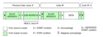
What we are trying to do is to read a single byte of data from a register (0x40) from the FPGA, using the FX3. The transaction should be as shown in the first image, where the FX3 does this steps:

1. Send start condition
2. Send the device address followed by a write bit
3. Receive an ACK from FPGA
4. Send register address (0x40)
5. Receive an ACK from FPGA
6. Send repeated start condition
7. Send device address followed by read bit
8. Receive ACK from FPGA
9. Receive byte from FPGA register
10. Send ACK to FPGA
11. Send stop condition to FPGA

The issue is that the FX3 does not release the Bus after sending the read address to the FPGA (step 7). This prevents the FPGA from sending the register data to the FX3 board. What could cause this problem?

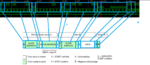
I have attached a second image that shows the result we get on the signal analyzer

Thanks
 

Attachments

  • Screenshot from 2020-07-17 17-16-52.png
    Screenshot from 2020-07-17 17-16-52.png
    31.2 KB · Views: 131
  • Annotation 2020-07-19 083101.png
    Annotation 2020-07-19 083101.png
    117.8 KB · Views: 134

Hi,

As far as I see the master does not release during data read from slave.
Released = high impedance (never HIGH, not LOW) so the external pullup causes a (weak) HIGH level.
But the master data line is LOW.

Generally: no data read is impossible. You will always get all bits (8 bits) of data unless the slave blocks the SCK line like in "clock stretching mode". But maybe the data you get is wrong

Klaus
 

It's not clearly explained what the traces in timing diagram mean. Considering that actual SDA state is wired "and" of master and slave, the diagram makes no sense. I'm not able to see that the master is blocking the bus.
 

I think what last fellow said is right.Perhaps,you need a pull-up resistor.With FPGA,you can set the SDA pin to weak pull-up state in EDA software which perhaps can be Quartus or Vivado.
 

I think what last fellow said is right.Perhaps,you need a pull-up resistor.With FPGA,you can set the SDA pin to weak pull-up state in EDA software which perhaps can be Quartus or Vivado.
The FPGAs I've used from both Intel and Xilinx have pull-up resistors in the range of 75K-150K I wouldn't use them to pull-up external board trace connections to multiple devices, they aren't designed as board level pull-ups.

I've seen this type of weak pull-up usage before and the aftermath where an external resistor ends up being blue wired onto the board to fix the lack of a physical pull-up resistor.
Perhaps having only one or two external devives on bus which need to be pull-up,in that situstion,the board do not need physical pull-up resistor .I have used that software weak pull-up in camera sensor communication two years ago and find it works well.So,can you describe the problem in a more detailed way.The problem perhaps refers to the board route destance or the number of devices on the bus.
 

Hi,

With that weak pull ups it surely may work. May. But don't be surprised if it does not work.

You simply have to keep on I2C standards and you have to keep on datasheet specifications regarding voltage levels, rise time and so on.
But also on noise immunity, stray capacitance, leakage currents .. that depend on location of your application. (Noise sources nearby, humidity...) and also on production tolerances of the devices and the PCB.

Many people think if a circuit is working for an hour, a week or even a year without fail it is a good and reliable design. I can't recommend this.

You may use a bungee rope that is designed for 150 pounds while your weight is 200 pounds. There is a good chance that it will carry you many jumps. But you have no guarantee. Humidity, ageing, temperature, jumping height....or buy a new, identical one with production tolerance. Good luck.

You are free to build and use anything you want, but please don't sell it.
Not as a air bag control, not as brake control, not as elevator control, but also not as cell phone that refuses to work when I get in trouble in the mountains (increased altitude, after a hit, modified temperature or humidity...). I even don't want it as coffee machine.

In my eyes there are already enough unreliable electronics around, I don't need new unreliable ones.

It's not only hobbyists that desingn this way, even big companies do. Some maybe out of laziness, others even knowingly..to make the products fail...

Klaus
 

Perhaps having only one or two external devives on bus which need to be pull-up,in that situstion,the board do not need physical pull-up resistor .I have used that software weak pull-up in camera sensor communication two years ago and find it works well.So,can you describe the problem in a more detailed way.The problem perhaps refers to the board route destance or the number of devices on the bus.
Go ahead and justify your bad design decision if you want, but it doesn't change the fact that it is wrong to rely on a variable sized non-compliant "weak" FPGA pull-up resistor that isn't meant to be a pull up for external devices. Given you are trying to justify that it works really shows that you don't know for sure and are just guessing it works because it worked on a lab unit or two.

Issues I have seen in the past include (on designs I had to fix)...
Poor rise time that exceeded the I2C requirements and another device on the bus failed to operate correctly because the FPGA pull-up was to "weak". A high level that wasn't very high due to bus capacitance loading the weak pull-up. Problems like that.

FPGA pull-ups are not there to pull up the external pin voltage (read the documentation if you don't believe this), they are designed to ensure the FPGA input buffers don't see intermediate (i.e. values near the voltage threshold that might cause the input buffer to oscillate). This is one of the reasons why they are all active prior to configuration of either Intel or Xilinx FPGAs and are enabled on unused input pins by default.
 

Hi,

With that weak pull ups it surely may work. May. But don't be surprised if it does not work.

You simply have to keep on I2C standards and you have to keep on datasheet specifications regarding voltage levels, rise time and so on.
But also on noise immunity, stray capacitance, leakage currents .. that depend on location of your application. (Noise sources nearby, humidity...) and also on production tolerances of the devices and the PCB.

Many people think if a circuit is working for an hour, a week or even a year without fail it is a good and reliable design. I can't recommend this.

You may use a bungee rope that is designed for 150 pounds while your weight is 200 pounds. There is a good chance that it will carry you many jumps. But you have no guarantee. Humidity, ageing, temperature, jumping height....or buy a new, identical one with production tolerance. Good luck.

You are free to build and use anything you want, but please don't sell it.
Not as a air bag control, not as brake control, not as elevator control, but also not as cell phone that refuses to work when I get in trouble in the mountains (increased altitude, after a hit, modified temperature or humidity...). I even don't want it as coffee machine.

In my eyes there are already enough unreliable electronics around, I don't need new unreliable ones.

It's not only hobbyists that desingn this way, even big companies do. Some maybe out of laziness, others even knowingly..to make the products fail...

Klaus
I have to say that I don't think what I saw before is true.So I asked you the differences yesterday.And I saw this kind of usage in the last company and didn't know that it is a bad design.

At last,thank you for telling me the problem that I haven't known yet.
--- Updated ---

Go ahead and justify your bad design decision if you want, but it doesn't change the fact that it is wrong to rely on a variable sized non-compliant "weak" FPGA pull-up resistor that isn't meant to be a pull up for external devices. Given you are trying to justify that it works really shows that you don't know for sure and are just guessing it works because it worked on a lab unit or two.

Issues I have seen in the past include (on designs I had to fix)...
Poor rise time that exceeded the I2C requirements and another device on the bus failed to operate correctly because the FPGA pull-up was to "weak". A high level that wasn't very high due to bus capacitance loading the weak pull-up. Problems like that.

FPGA pull-ups are not there to pull up the external pin voltage (read the documentation if you don't believe this), they are designed to ensure the FPGA input buffers don't see intermediate (i.e. values near the voltage threshold that might cause the input buffer to oscillate). This is one of the reasons why they are all active prior to configuration of either Intel or Xilinx FPGAs and are enabled on unused input pins by default.
First,thank you for your reply that I have known a lot from it.And I really don't know the difference between the two kind of pull-up.

Can you recommand some books about FPGA for I really lack the knowledge about it.I have only one year experience in FPGA design,and had not learnt the necessary knowledge in the last company,because last company doesn't have good documents or books.I have learnt FPGA nearly on myself and the self-study has been too exhausting,hard and disorder.
 
Last edited:

You learn how to use a vendors FPGA by reading the 1000s of pages of documentation published by Xilinx, Intel, Microsemi, etc or taking training classes offered by the vendors themselves. You don't learn FPGAs by reading something your last company wrote up. Your typical so called company "expert" is usually the engineer that used an FPGA (doesn't matter if they used it correctly or not).

Not sure what you mean by two kinds of pull-ups (internal/external?). For pullups consider that V/R is the current required to pull the pin down to GND, so a very large R means a very weak pullup and very little current is needed to pull the pin down, which is why I would not recommended to pull-up an external trace and another pin.
 

Hi,

And I really don't know the difference between the two kind of pull-up.
The problem is not "internal" or "external" pull up.
The problem simply is the "value" ... to meet specified rise time and voltage levels.

An example: You could use the FPGA internal pull up to limit a LED current ...
I doubt one is satisfied with the result. The reason is the same as with the I2C bus: The current is too low to usefully drive the LED.
The difference is: with a LED you get immediate optical feedback that the current is too low.
With the I2C bus you need a scope to see this.

Klaus

Added: The FPGA internal pull up mainly is used to prevent signal lines from floating.
Here especially with
* unused Pins
* input pins that may be diconnected
* tri state busses
Floating signals may cause oscillations, increases EMI/EMC problems, increased supply current.
 
Last edited:

You learn how to use a vendors FPGA by reading the 1000s of pages of documentation published by Xilinx, Intel, Microsemi, etc or taking training classes offered by the vendors themselves. You don't learn FPGAs by reading something your last company wrote up. Your typical so called company "expert" is usually the engineer that used an FPGA (doesn't matter if they used it correctly or not).

Not sure what you mean by two kinds of pull-ups (internal/external?). For pullups consider that V/R is the current required to pull the pin down to GND, so a very large R means a very weak pullup and very little current is needed to pull the pin down, which is why I would not recommended to pull-up an external trace and another pin.
Hi

Perhaps,I'm too lazy and want to make few efforts to get more knowledge or finish the work.But,at the same time,work can be urgent and I don't know the proper learning order and don't have enough time.These are big problems when one graduate from university 、is not very familar with FPGA and can't get initial train from company.
--- Updated ---

I doubt one is satisfied with the result. The reason is the same as with the I2C bus: The current is too low to usefully drive the LED.


Hi,

How can I solve this problem for there is only one engineer using FPGA,and that guy is me.I don't know too many things.:cry:
 
Last edited:

Perhaps,I'm too lazy and want to make few efforts to get more knowledge or finish the work.But,at the same time,work can be urgent and I don't know the proper learning order and don't have enough time.These are big problems when one graduate from university 、is not very familar with FPGA and can't get initial train from company.

How can I solve this problem for there is only one engineer using FPGA,and that guy is me.I don't know too many things.:cry:
You should be reading the documentation at home to learn about the FPGA device. The company is paying you to get a job done, not learn about FPGAs. You only need to refer to the documentation at work to refresh your memory or to verify some detail.

Engineering is a life long career of learning new things as technology moves forward. You can't escape having to learn new stuff and most of that learning isn't going to happen during your 9-5 work day. So either get used to spending time outside work studying or switch to a non-technical role where you can spend all of your free time outside work socializing.

You better decide now if you would rather have a social life or a career you excel at.
 
Hi,
Engineering is a life long career of learning new things as technology moves forward.
I fully agree.
For sure you can't know anything from school. And you can't learn all in the first month or first year.

Klaus
 
You should be reading the documentation at home to learn about the FPGA device. The company is paying you to get a job done, not learn about FPGAs. You only need to refer to the documentation at work to refresh your memory or to verify some detail.

Engineering is a life long career of learning new things as technology moves forward. You can't escape having to learn new stuff and most of that learning isn't going to happen during your 9-5 work day. So either get used to spending time outside work studying or switch to a non-technical role where you can spend all of your free time outside work socializing.

You better decide now if you would rather have a social life or a career you excel at.
Hi

In fact,I have spent much money and time on FPGA.What I want to say is that self-study can be very difficuit for a freshman in this field ,and he or her ,at the same time has a urging work to do.In our country,designing is a very fast thing that self-study can't cover the necessary knowledge or skills.For me,encoutering a problem,I have nobody to ask for advice in the company or my circumstance.That is the reason why I have to find website like this to get knowledge or help.

When I get home,it is always seven or eight clock and I'm too tired to read a book.
--- Updated ---

Hi,

I fully agree.
For sure you can't know anything from school. And you can't learn all in the first month or first year.

Klaus
I agree.But,in first year,the company seems unwilling to teach freshman some knowledge when other companys would teach the freshman for three or six months.
 
Last edited:

When I get home,it is always seven or eight clock and I'm too tired to read a book.
--- Updated ---


I agree.But,in first year,the company seems unwilling to teach freshman some knowledge when other companys would teach the freshman for three or six months.
Sounds like you work at a sweat shop.

Companies, like where you appear to work at, don't care if you burn out because they can just hire another new grad to take your place. Only the workaholics will survive in such places. Your choices are find another job, suffer premature burn out (and maybe have to leave the field of engineering), or become a workaholic to be successful at that company.
 

In fact,I have spent much money and time on FPGA.What I want to say is that self-study can be very difficuit for a freshman in this field ,and he or her ,at the same time has a urging work to do.In our country,designing is a very fast thing that self-study can't cover the necessary knowledge or skills.For me,encoutering a problem,I have nobody to ask for advice in the company or my circumstance.That is the reason why I have to find website like this to get knowledge or help.
That is why we have specific forums. This forum and also there is Xilinx and Intel FPGA forums where even basic questions are answered IF THEY ARE ASKED IN A PROPER MANNER with supporting stuff.
 

Sounds like you work at a sweat shop.

Companies, like where you appear to work at, don't care if you burn out because they can just hire another new grad to take your place. Only the workaholics will survive in such places. Your choices are find another job, suffer premature burn out (and maybe have to leave the field of engineering), or become a workaholic to be successful at that company.
Actually,the last company I worked in requested that we had to work from 8:30 AM to 9 PM for 3 days and from 8:30 AM to 5:30 PM for 3 days in a week.Even when I was ready to sleep at 11 or 12 PM,the manager could call me to talk about work.Work can be pushing,and pressure was very large.So,I don't have that sweat shop.When I quit from the company,I am very weak,exhausted and angry.
 

Actually,the last company I worked in requested that we had to work from 8:30 AM to 9 PM for 3 days and from 8:30 AM to 5:30 PM for 3 days in a week.
Terrible....... Sounds like a Japanese/Korean company located in Japan/Korea!
It is not possible even to imagine of such a work cultute in Europe/America.
 

Terrible....... Sounds like a Japanese/Korean company located in Japan/Korea!
It is not possible even to imagine of such a work cultute in Europe/America.
The day has gone.Things now are better.I choose to work in another city.And I avoid working in the company like that.
 

Status
Not open for further replies.

Part and Inventory Search

Welcome to EDABoard.com

Sponsor

Back
Top