Continue to Site

Welcome to EDAboard.com

Welcome to our site! EDAboard.com is an international Electronics Discussion Forum focused on EDA software, circuits, schematics, books, theory, papers, asic, pld, 8051, DSP, Network, RF, Analog Design, PCB, Service Manuals... and a whole lot more! To participate you need to register. Registration is free. Click here to register now.

Huge discrepancies between schematic and momentum in ADS (2016)

Status
Not open for further replies.

Hilbertstrauss

Newbie level 5
Joined
Jan 1, 2019
Messages
9
Helped
0
Reputation
0
Reaction score
0
Trophy points
1
Activity points
205
Greetings,

I tried to simulate the simple following power divider in schematic in ADS 2016,
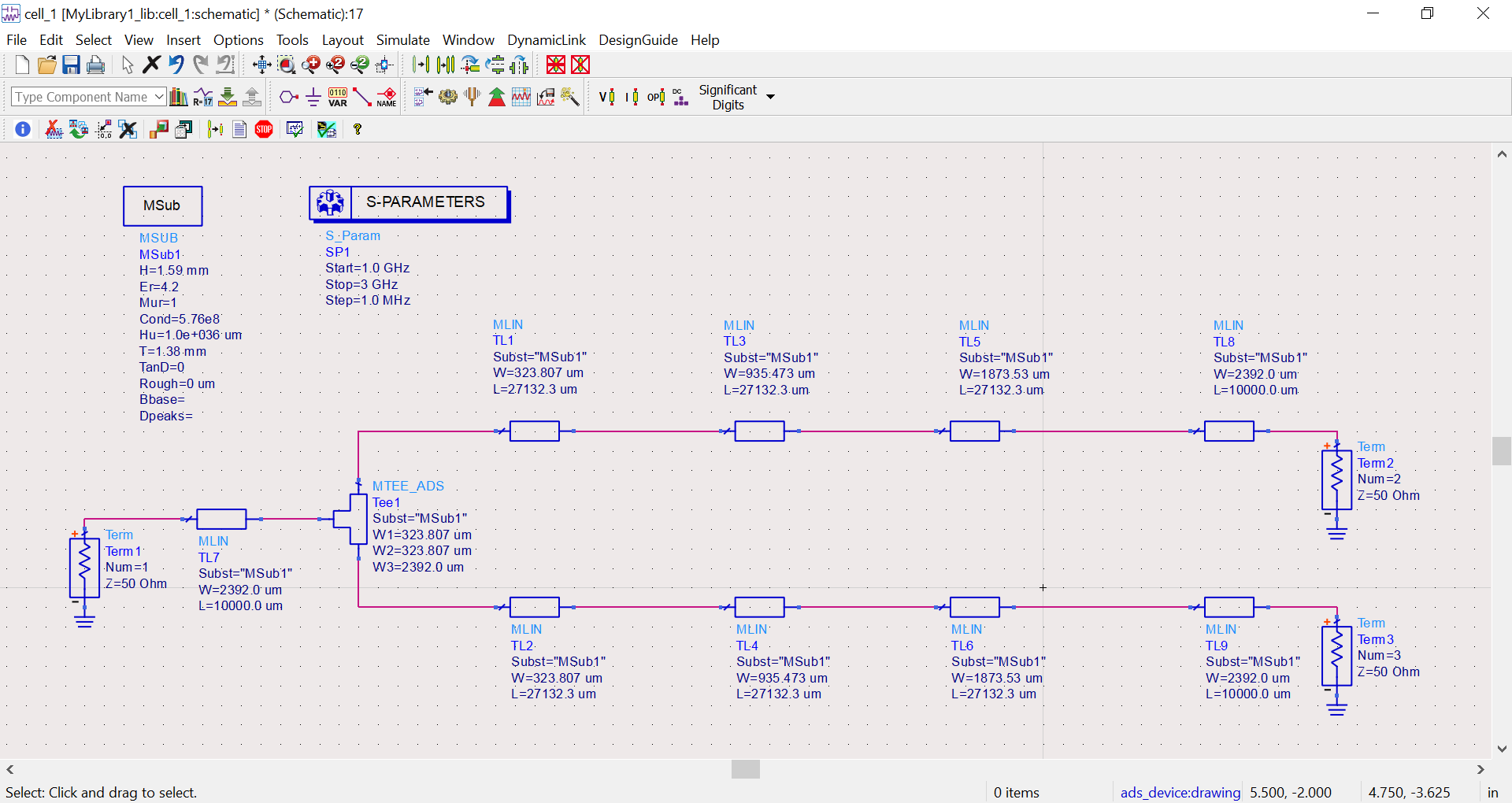
schematic.PNG


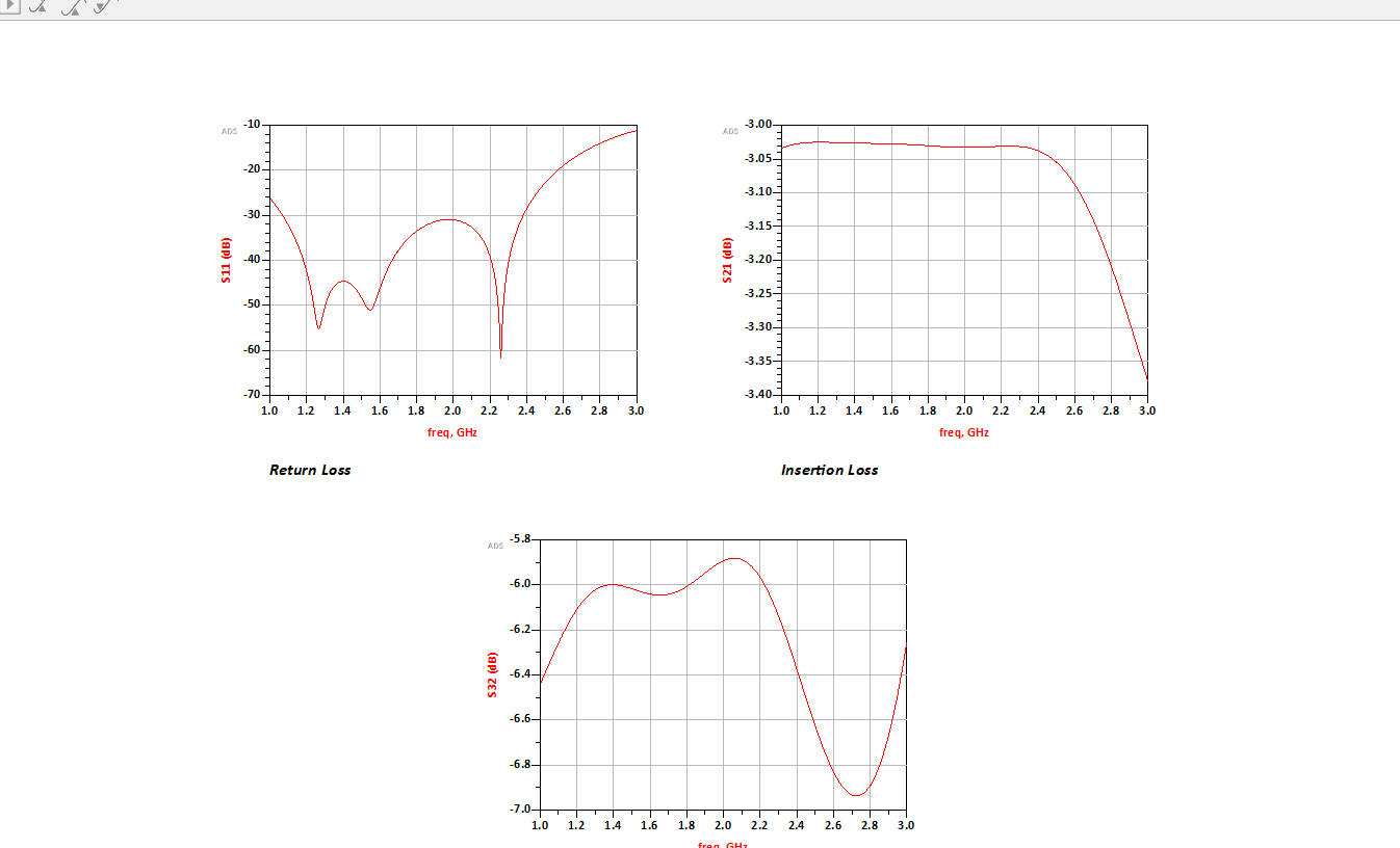
I got the following s parameters,

schem.PNG


Then I made the same circuit in layout and run a momentum microwave simulation,
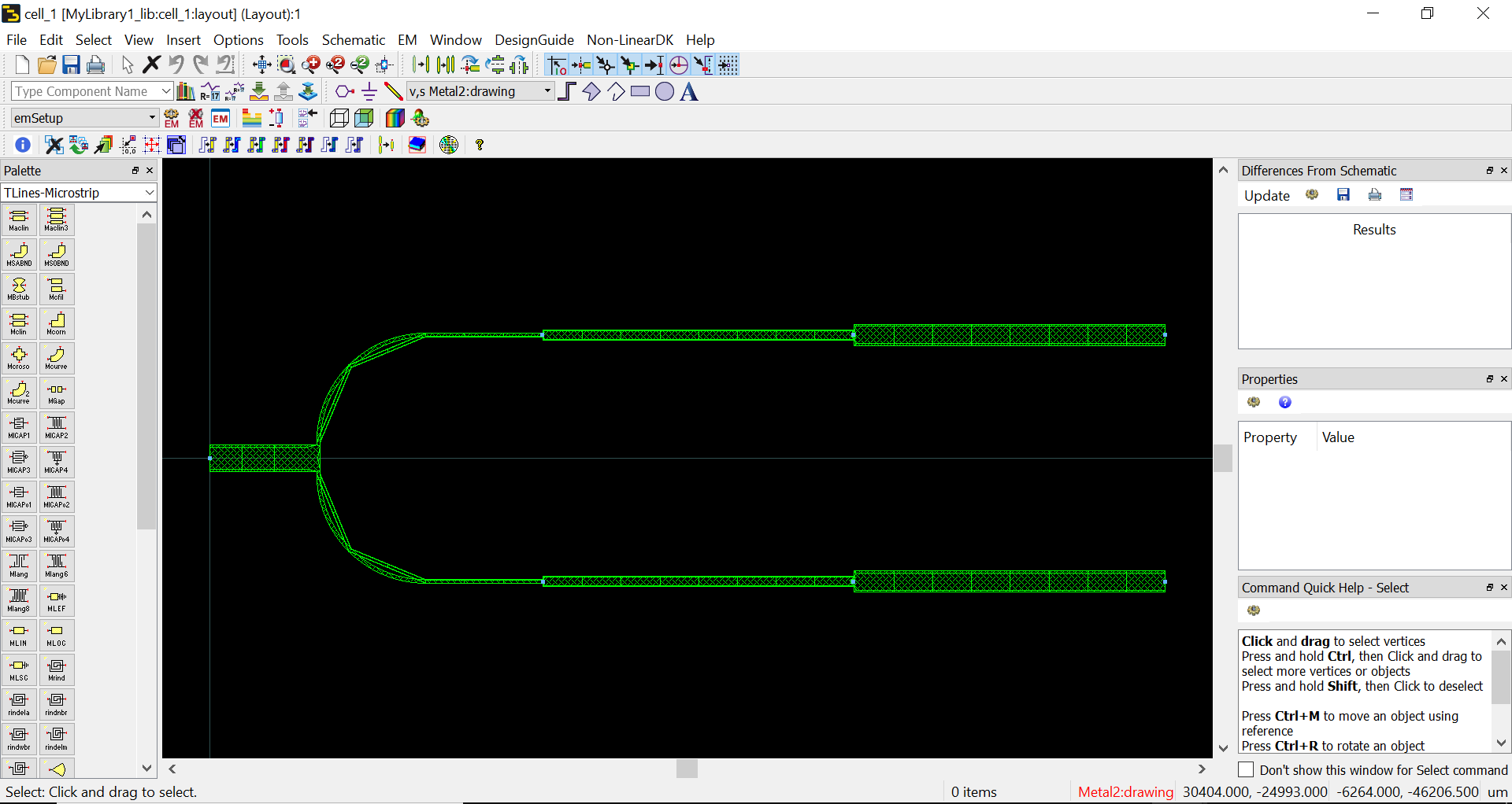

layout.PNG


As you can see, the results were very different from those obtained using schematic,
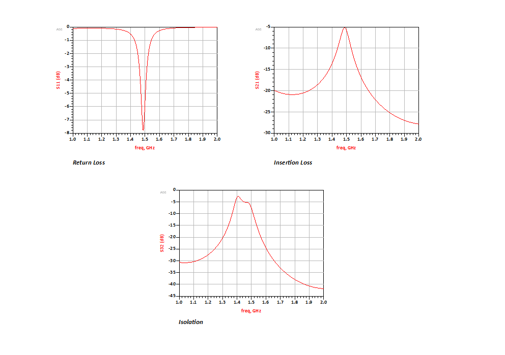
lay.PNG


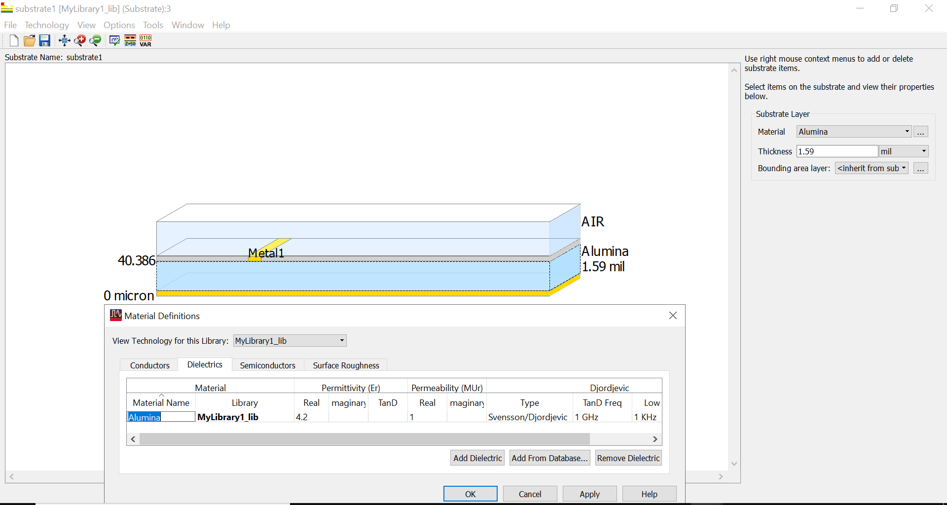
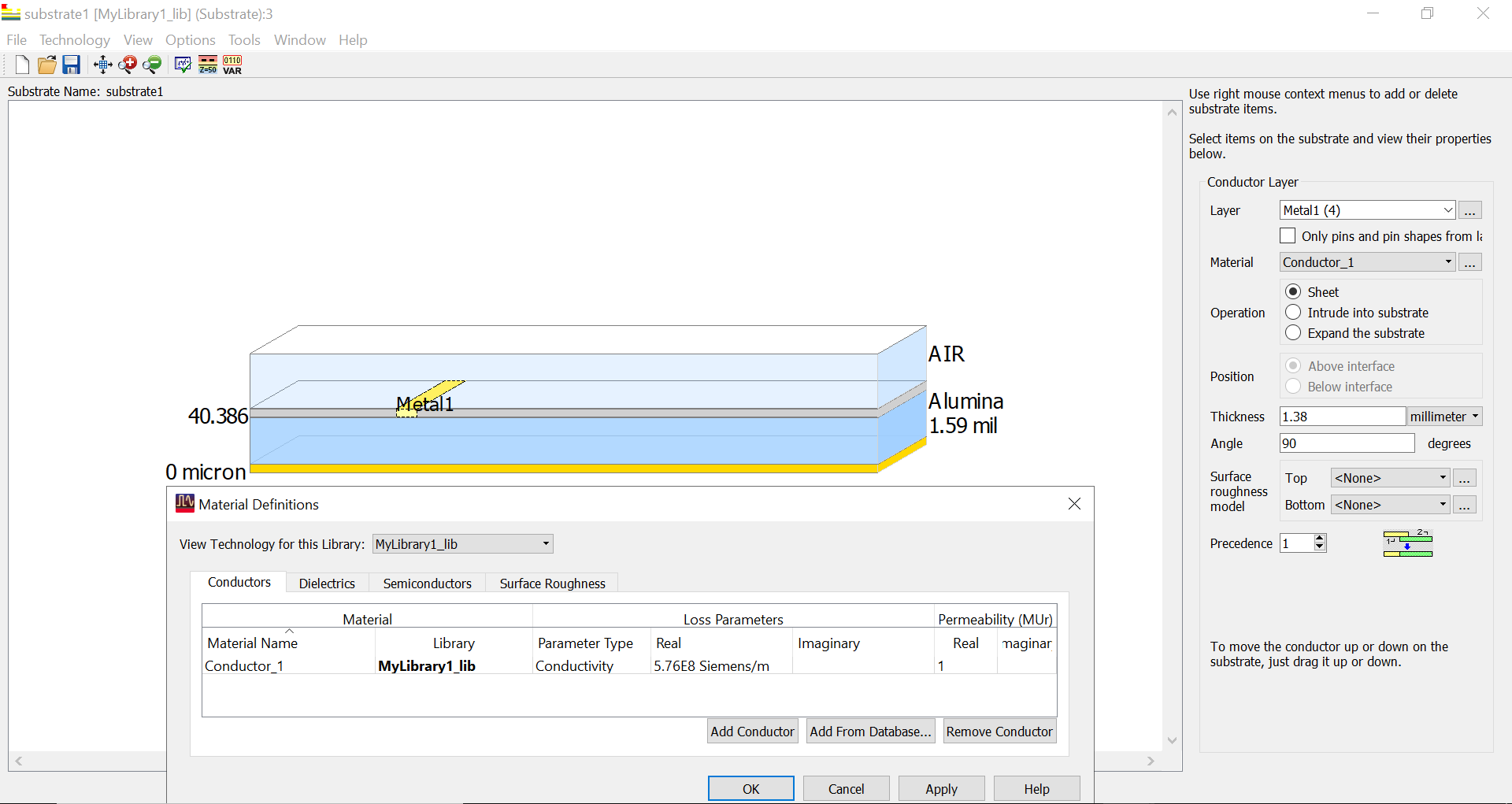
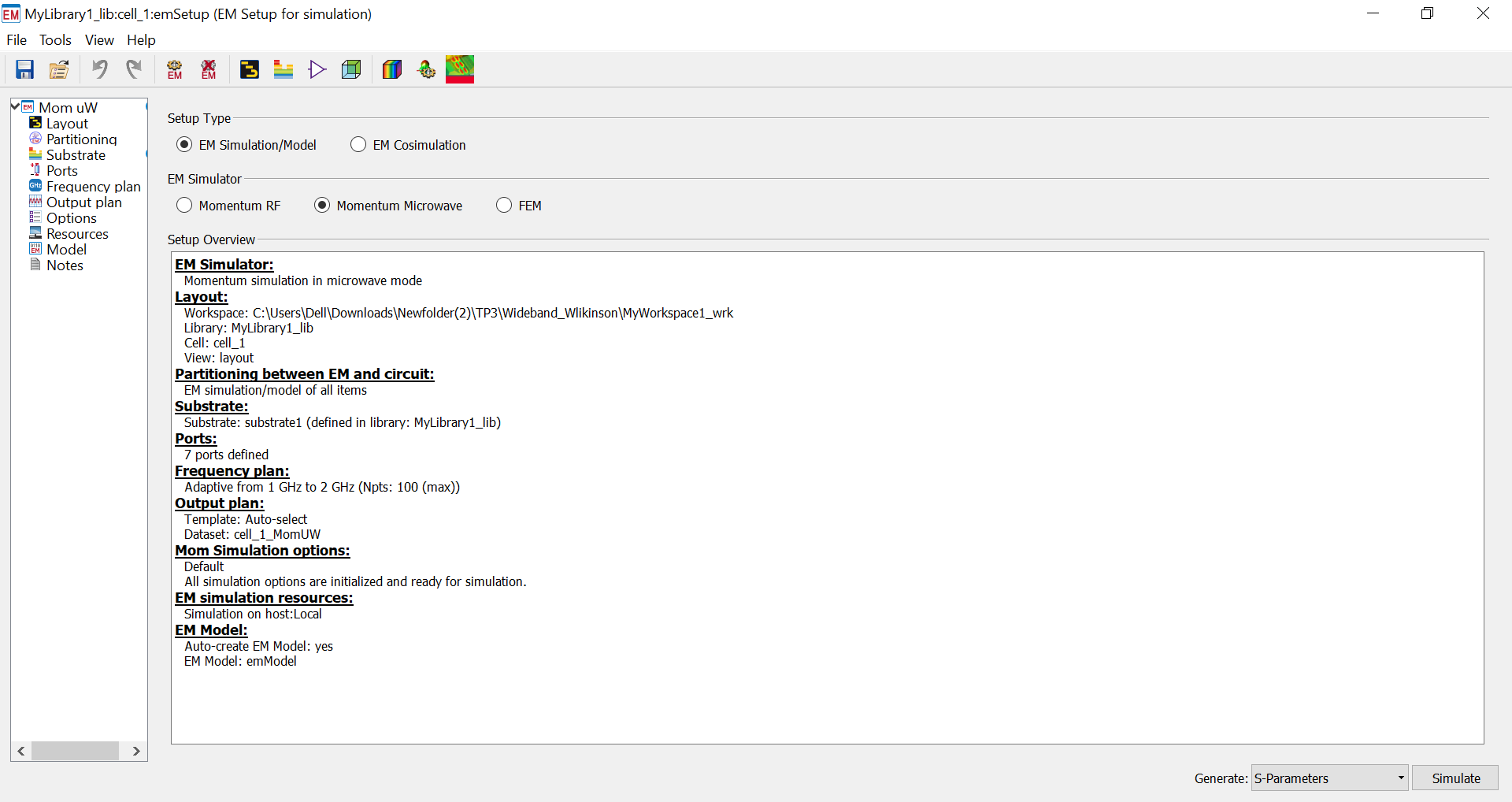
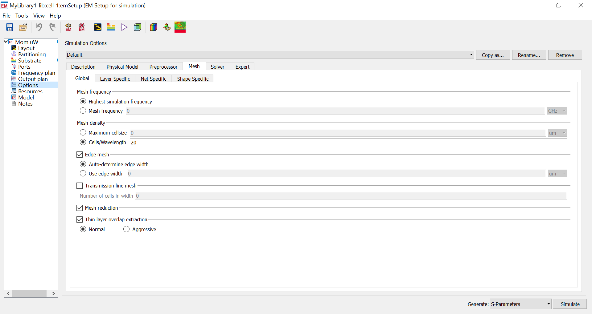
What might cause the momentum simulation parameters/design to give results that are so different from those obtained with schematic? I used the following settings:

1.PNG


2.PNG


3.PNG


4.PNG


5.PNG


If needed, the workspace folder can be found here: https://drive.google.com/file/d/135CLcoooKmi5xk7iEFp4FcsDqI3TENIO/view?usp=sharing

Thank you!
 
Last edited:

Check your units!!!

In the schematic MSUB you have H=1.59 mm but in the EM setup your substrate (Alumina) thickness is set as 1.59 mil. These are not the same, 1 mm is not equal to 1 mil (1 mil = 0.001 inch, 1 mm = 39.37 mil).

Also your conductor thickness which is set as 1.38 mm seems unusually large. 1oz copper on PCBs is more like 1.38 mil (35 um or 0.035 mm). Again check your units.

There are other issues like the EM mesh but that would be fine tuning once the material data is set correctly.
 
Not only the units are wrong, but also you missed in Momentum the TL8 and TL9 from the schematic.
 
Another mistake (less effect) is that your Momentum preprocessing of geometries simplifies the curves to straight lines. You can see that difference between layout and meshed view in the screenshot. Set less aggressive geometry simplification.

Also, your schematic simulation does not have MSTEP elements, which calculate the effect from a step in width between lines. You will have more accurate schematic model results when adding the MSTEP elements.
 
Also you used mesh reduction but it's not efficient for this kind of curved planar structures.
Deselect this option and increase mesh density.
 
Status
Not open for further replies.

Part and Inventory Search

Welcome to EDABoard.com

Sponsor

Back
Top