Continue to Site

Welcome to EDAboard.com

Welcome to our site! EDAboard.com is an international Electronics Discussion Forum focused on EDA software, circuits, schematics, books, theory, papers, asic, pld, 8051, DSP, Network, RF, Analog Design, PCB, Service Manuals... and a whole lot more! To participate you need to register. Registration is free. Click here to register now.

[HSPICE] Simple PMOS Question

Status
Not open for further replies.

MammPp

Junior Member level 2
Joined
Sep 14, 2008
Messages
22
Helped
0
Reputation
0
Reaction score
0
Trophy points
1,281
Activity points
1,441
Hi all,

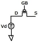
I tried to use HSPICE to simulate the regular PMOS circuit,

However, my problem is, why does source voltage is equal to 1V when gate voltage is equal to 1V.

The following is my code

Thank you so much for your help

Best
PJ

Test
.include 'PMOS 45nm.txt'

.param Vd = 1V

Vsupply 1 0 Vd


Mp D Gb S 1 PMOS L=0.25u W=1u

Vd D 0 DC Vd
Vin Gb 0 pulse (Vd 0 step 0.001ns 0.001ns step 'step*2')

.PARAM step = 300ns

.tran 1ns 'step*3'

.option post = 2
.op
.end
 

... why does source voltage is equal to 1V when gate voltage is equal to 1V.
Both source & drain voltages are equal to 1V :
.param Vd = 1V
Vsupply 1 0 Vd
Vd D 0 DC Vd

Mp D Gb S 1 PMOS L=0.25u W=1u
The source node (S) is still floating. You could either replace it by "1" (like the bulk node, which is supplied by Vsupply), or you need another connection (short circuit between S and node "1") :
Vsource S 1 0V

But still source and drain are at the same voltage level. Don't know if you would want that!?

Vin Gb 0 pulse (Vd 0 step 0.001ns 0.001ns step 'step*2')
This pulses your PMOS from a diode connected configuration (Vgs=Vds = 0V)
to Vgs=-1V (but still Vds=0V, so no current flow, either).

I'd suggest that you should change the Vsupply to 2V :
Vsupply 1 0 '2*Vd'
Then your drain voltage is 1V (Vds=-1V), and with your present gate pulse source you switch your PMOS between its diode connected configuration (Gb=Vd) , or Vgs=Vds = -1V , i.e. saturation region) and its "fully on" configuration (Gb=0 , resp. Vgs=-2V). Don't know if this is your intention?
 
  • Like
Reactions: MammPp

    MammPp

    Points: 2
    Helpful Answer Positive Rating
Thank you for your answer erikl

I am not really understand your answer
However, I attach picture of my model that I simulated.

Since I would like to check that PMOS could pass the VDD or not, this circuit is generated. By check the voltage at node S, when GB = 1V (or Vd). In my view, when GB is 1V, voltage at node S should be zero, am I correct ?

However, the simulation result that I got is 1V ??

I wondered, what's wrong with my model
 

Attachments

  • HSPICE Question.jpg
    HSPICE Question.jpg
    4.3 KB · Views: 84

Interestingly, when the gate voltage is 0 volt, then the node S will pull up to the 1volt(transistor acts as a switch). This voltage is stored on the parasitic cap which exists on node S. When you turn off the transistor (Vgate=1),the charges on node S can not scape and you always will see the constant voltage at node S.
That's the reason.

By the way this circuit is a simple sample and hold.
 
  • Like
Reactions: MammPp

    MammPp

    Points: 2
    Helpful Answer Positive Rating
Hi Milad-D,

I understand your point, but the thing is at the first simulation which gate voltage is 1V, voltage at node S is 1V.
To make it more simple, I change the gate voltage to

Vin Gb 0 DC Vd

The result is voltage at node S is 1V.
 

The simulator does an initial DC analysis to determine the initial voltages at all nodes.
It determines it as 1V, that's all.
As S is a high impedance node, it's voltage is dependent on parasitics and leakages. It so happens that the simulator calculates it as 1V!
If you want it to be 0V, you should put either a pull-down transistor, or a resistive load.

Or if you want a more realistic scenario, ramp your vdd instead, and pass your vin through a couple of inverters.
 
Last edited:
  • Like
Reactions: MammPp

    MammPp

    Points: 2
    Helpful Answer Positive Rating
Thank you so much for your help checkmate,

Now it's worked and it's clear for me :D
 

Status
Not open for further replies.

Part and Inventory Search

Welcome to EDABoard.com

Sponsor

Back
Top