BackerShu
Member level 3
reltol vabstol sigma delta
Hi, everyone. A question about specifying the 2rd sigma delta modulator bothers you.
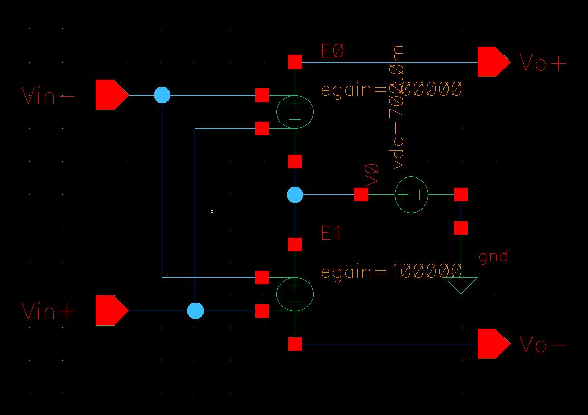
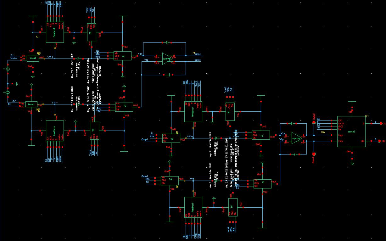
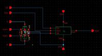
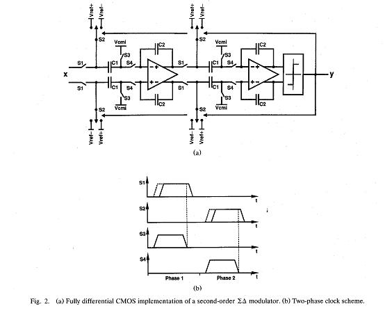
The modulator that I chose is shown in Fig 1:

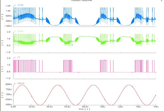
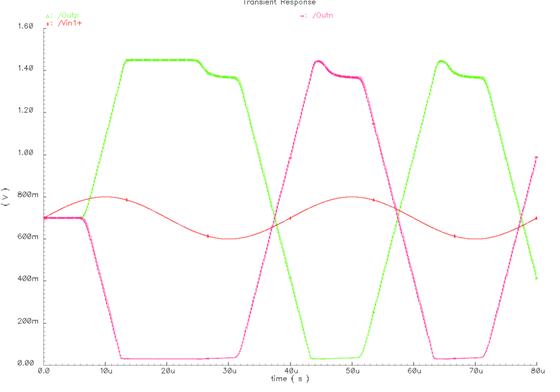
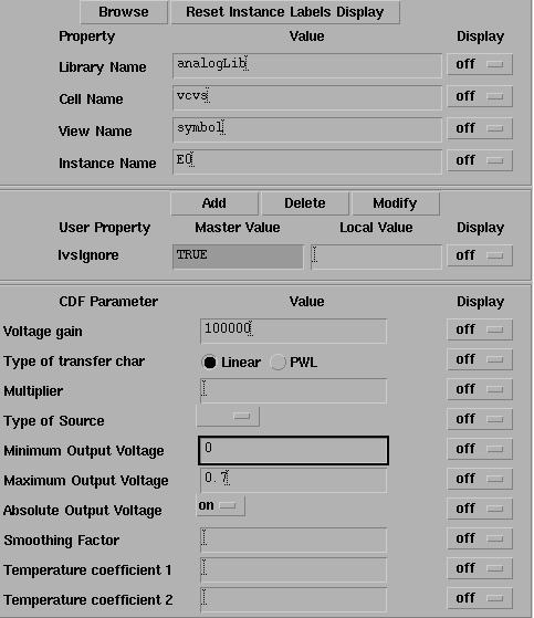
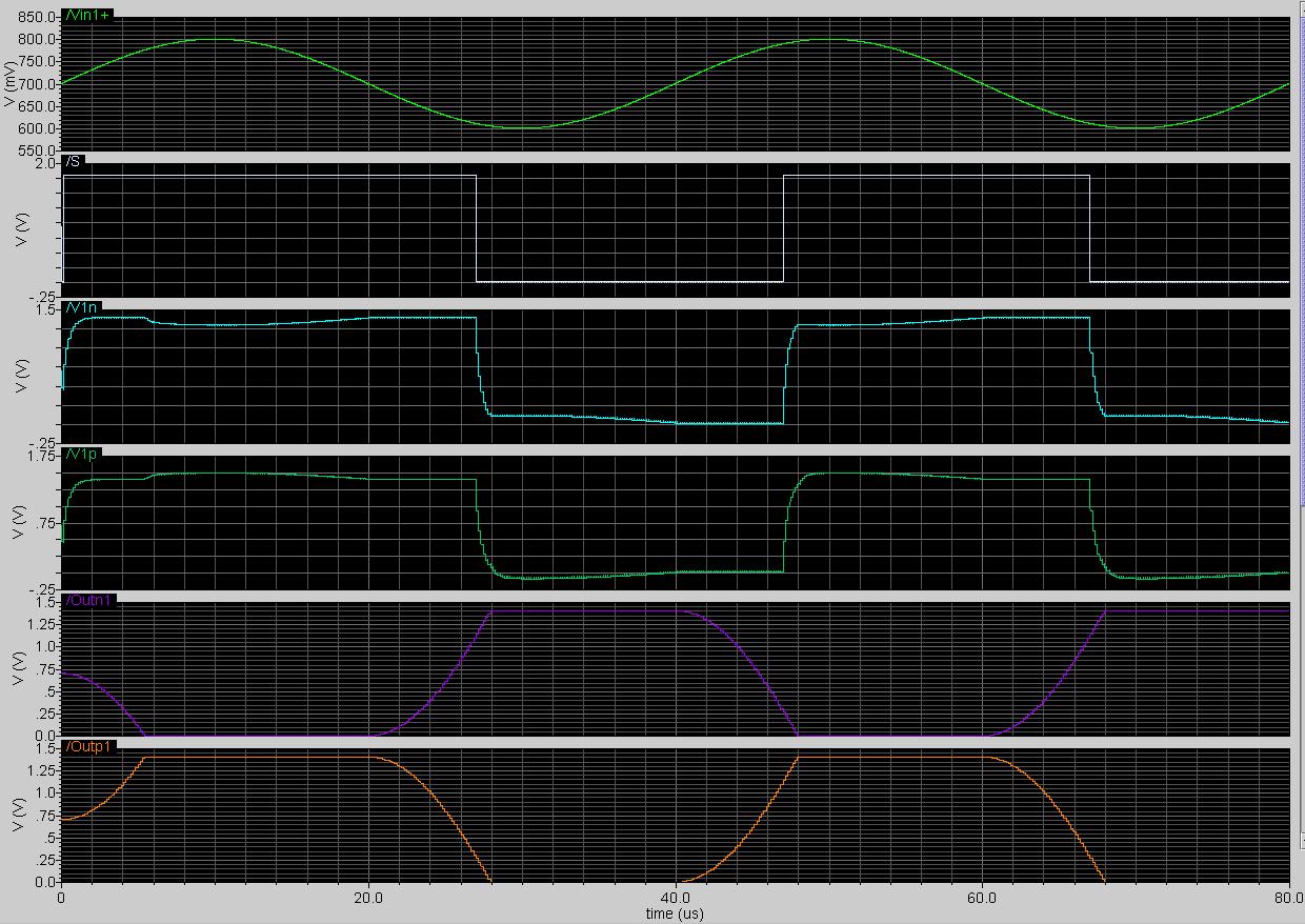
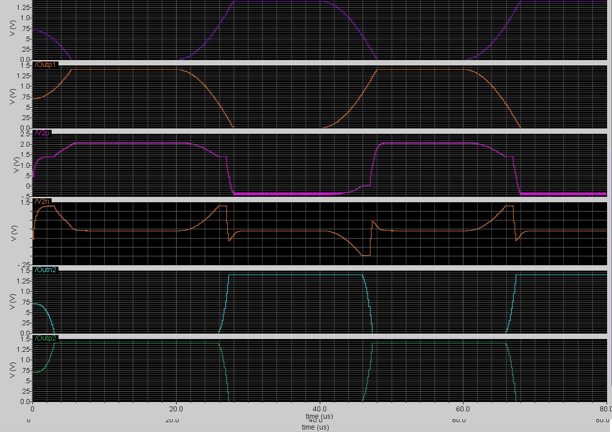
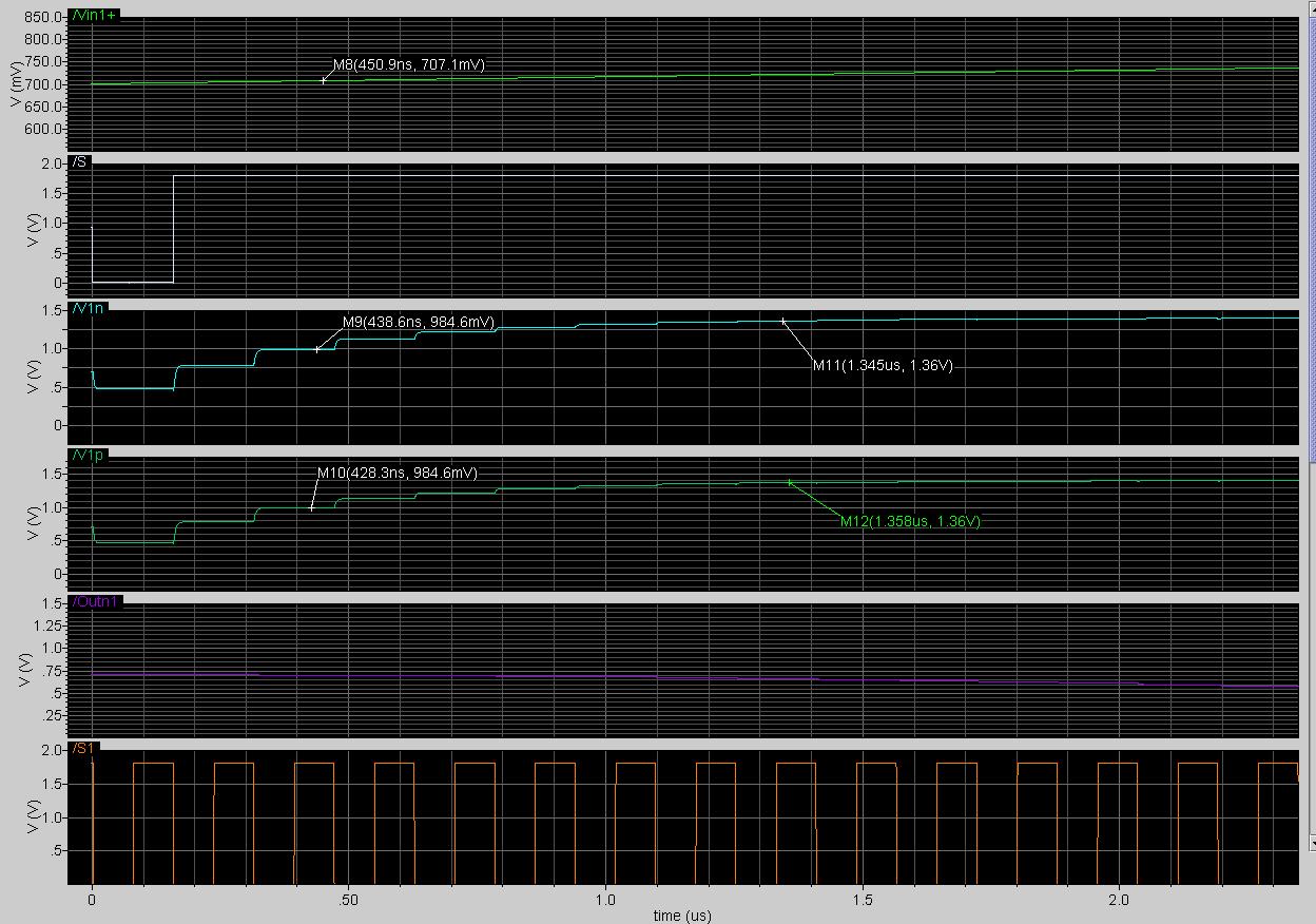
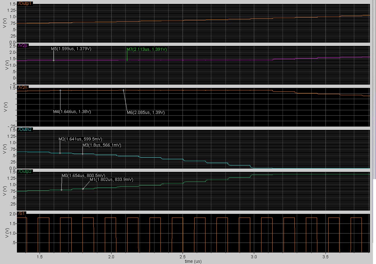
Here are somethings about the amplifer(or integrator) and comparator. The supply voltage of the modulator is 1.8V
Amplifiers: the input common mode voltage is 0.7V,and the output voltage range is 0-1.4v. The integrator's gain is 1/2. The two stages integrator works well when I set Vcmi 0.7v and using 0v to substitute the feedback voltage Vref+ and Vref-.
Comparator: It works well on the sample clock 6.4MHz.
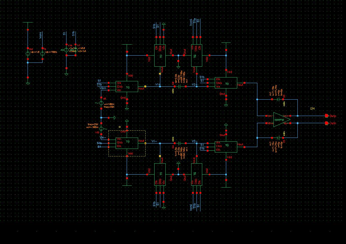
At last, I connect the all the parts to check whether the modulator works. The feedback circuit I design is shown in Fig2.
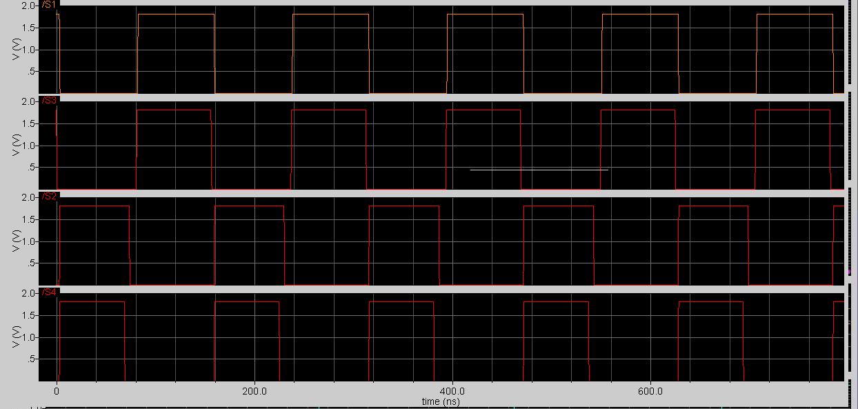
Where R and S are the output of the comparator,S2 and S2b are the clock signal,and symbol TG is a simple CMOS switch.
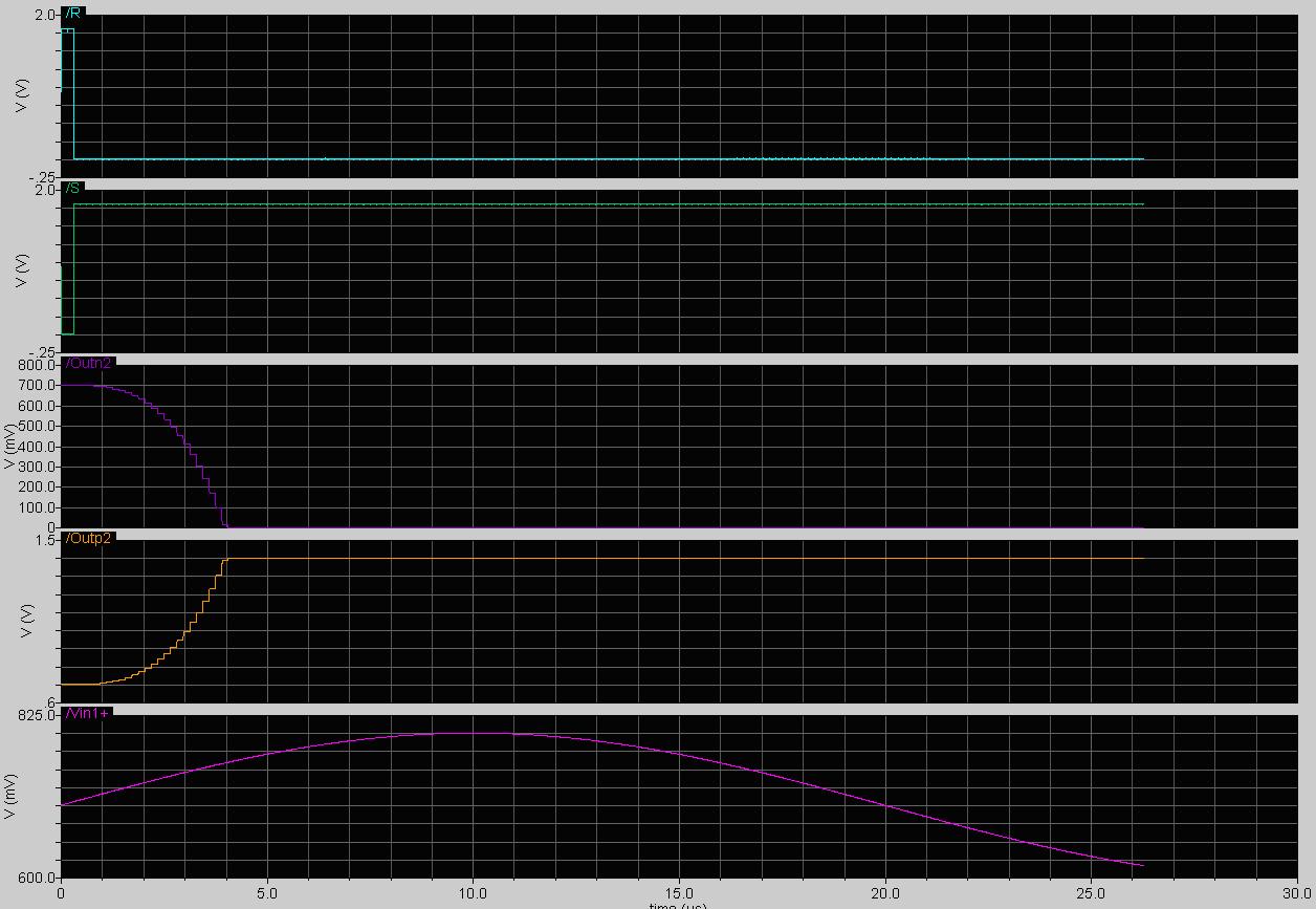
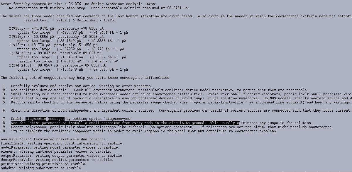
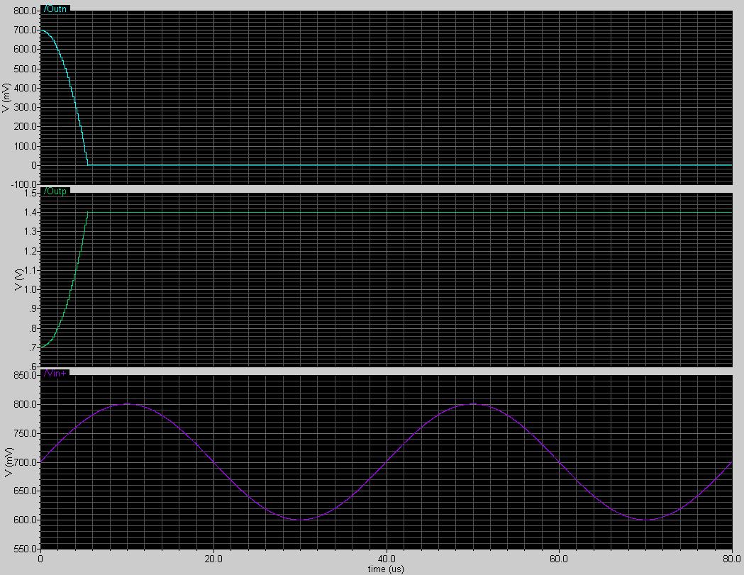
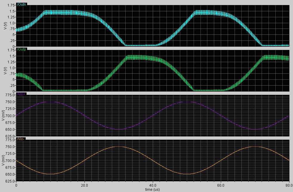
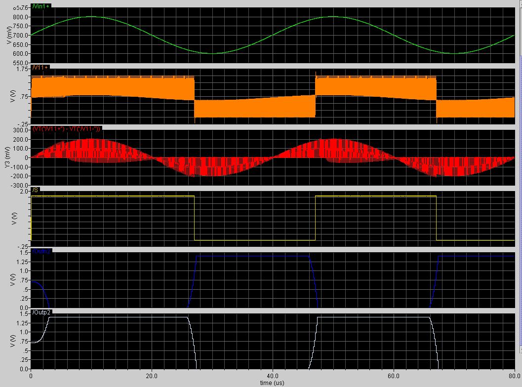
In the simulation, I set Vref+ 1.4v,Vref- 0v and Vcmi 0.7v.But the modulator's performance isn't right.I think the problems may lie in this two aspects.
1) I set the wrong value of Vref+ Vref- and Vcmi
2) The feedback that I decide isn't suitable for the modulator.
Please help me! Thank you in advance!
Regards!
BackerShu
Hi, everyone. A question about specifying the 2rd sigma delta modulator bothers you.
The modulator that I chose is shown in Fig 1:
Here are somethings about the amplifer(or integrator) and comparator. The supply voltage of the modulator is 1.8V
Amplifiers: the input common mode voltage is 0.7V,and the output voltage range is 0-1.4v. The integrator's gain is 1/2. The two stages integrator works well when I set Vcmi 0.7v and using 0v to substitute the feedback voltage Vref+ and Vref-.
Comparator: It works well on the sample clock 6.4MHz.
At last, I connect the all the parts to check whether the modulator works. The feedback circuit I design is shown in Fig2.
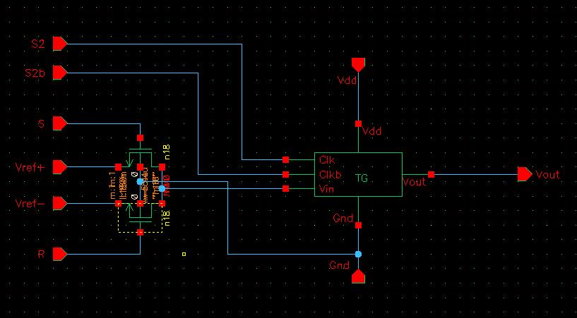
Where R and S are the output of the comparator,S2 and S2b are the clock signal,and symbol TG is a simple CMOS switch.
In the simulation, I set Vref+ 1.4v,Vref- 0v and Vcmi 0.7v.But the modulator's performance isn't right.I think the problems may lie in this two aspects.
1) I set the wrong value of Vref+ Vref- and Vcmi
2) The feedback that I decide isn't suitable for the modulator.
Please help me! Thank you in advance!
Regards!
BackerShu