david0632
Newbie
Hi, everyone:
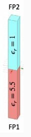
I am using the CST (unit_cell&open boundary&Fsolver) to simulate the refletion of dielectric interface. The plane wave is propatating from the space of dielectric of permittivity 5.5 to the one of permittivity 1.
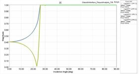
But when the incident angle is larger than the critical angle, the error happens: "The material in port Zmax corresponds to a scan angle outside the visible space. Please change the background material to the material with the lowest product of relative permeability and relative permittivity (the lowest refraction index), or use periodic boundaries with the phase specified rather than the scan angle".
Can anyone give me some hints? Thank you very much!!
PS: There is a similar problem in HFSS, and Joaonizer gave the solution through changing the background material. Unfortunately, the solution does not apply to the CST configuration. (https://forum.ansys.com/forums/topi...ion-dielectric-interface-boundary-conditions/)
I am using the CST (unit_cell&open boundary&Fsolver) to simulate the refletion of dielectric interface. The plane wave is propatating from the space of dielectric of permittivity 5.5 to the one of permittivity 1.
But when the incident angle is larger than the critical angle, the error happens: "The material in port Zmax corresponds to a scan angle outside the visible space. Please change the background material to the material with the lowest product of relative permeability and relative permittivity (the lowest refraction index), or use periodic boundaries with the phase specified rather than the scan angle".
Can anyone give me some hints? Thank you very much!!
PS: There is a similar problem in HFSS, and Joaonizer gave the solution through changing the background material. Unfortunately, the solution does not apply to the CST configuration. (https://forum.ansys.com/forums/topi...ion-dielectric-interface-boundary-conditions/)