Continue to Site

Welcome to EDAboard.com

Welcome to our site! EDAboard.com is an international Electronics Discussion Forum focused on EDA software, circuits, schematics, books, theory, papers, asic, pld, 8051, DSP, Network, RF, Analog Design, PCB, Service Manuals... and a whole lot more! To participate you need to register. Registration is free. Click here to register now.

How to simulate GDSII/Gerber/DXF file in ADS Layout ?

Status
Not open for further replies.

Sri Harsha

Junior Member level 2
Joined
Apr 21, 2014
Messages
24
Helped
0
Reputation
0
Reaction score
0
Trophy points
1,281
Activity points
1,445
Hi friends,

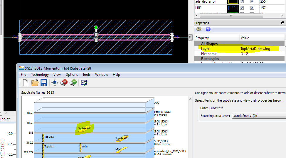
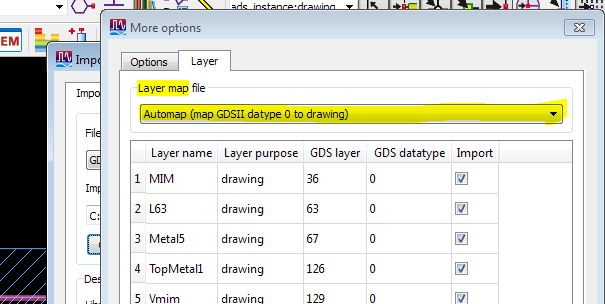
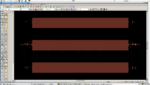
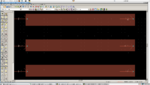
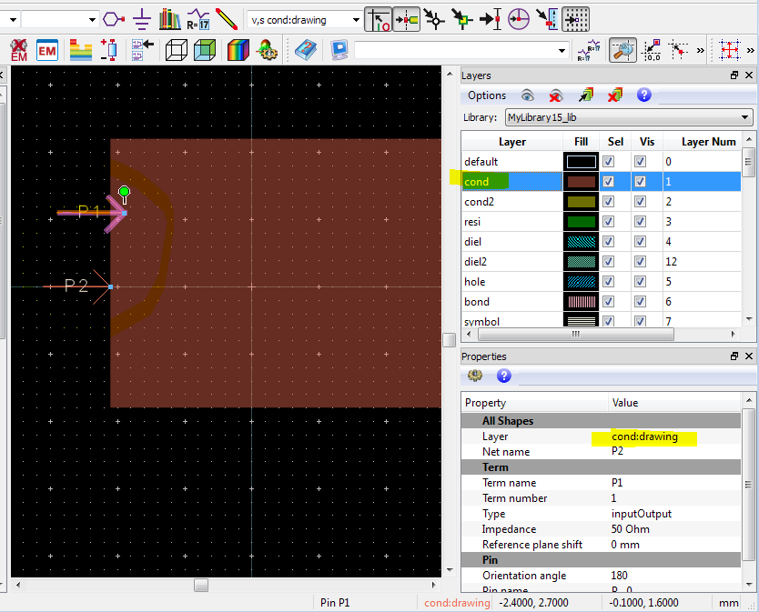
How to simulate gdsii/gerber file in ads layout, for example I designed some X in ADS layout and I generated the gerber/gdsii file for that and if i want to simulate the design by importing into ads layout I am unable to add ports for that even though after importing it is not asking about layer information but I gave as cond...problem not solved. so can anybody please suggest me to solve this issue.


Thanks and Regards,

SriHarsha Vardhan
 

I believe you can do a Co-Simulation or a Momentum Simulation. Both subjects are well documented in ADS.
 

simulate the design by importing into ads layout

I answered your question in ADS forum, but it seems that you misunderstood the answer.

Problem: If you import your Gerber/GDSII, the default is that imported metal is on new layers (not on cond). These new layers are not included in EM simulation, because the default EM substrates only map layer "cond".

Solution: During import, click on the Options button to see the layer names that will be used. After import, open the EM substrate editor and map your imported metal layers (layer names) as metal or vias.

You can also see the layer of an object in the properties window (View > Properties Window). This layer must be included in your EM substrate (EM stackup), otherwise the metal will be ignored for EM.

 
Hello sir,

I understood and I am trying to do that also, but in importing once i am trying to give layer information there is no .map file created in my library then I thought of changing that but I am unable to add layer, so can you pls see the below images once.and i ma using only one substrate that is FR4
 

Attachments

  • 1.png
    1.png
    235.7 KB · Views: 187
  • 2.png
    2.png
    229.5 KB · Views: 146

but in importing once i am trying to give layer information there is no .map file created in my library

Yes, you need to create the mapping manually with the buttons at the bottom
or
just use the drop-down list and switch to auto-mapping.

 
Thank you somuch for your reply sir,

pls find the below images I gave my substrate details and that what I got in automap everything I did but eventhough I created layer as cond it is default, so from the morning I am getting the same as layer definition file not found, importing is done but i am unable to give port to that, can you pls describe me step by step if possible with images
 

Attachments

  • substrate.png
    substrate.png
    149 KB · Views: 146
  • automap.png
    automap.png
    141.4 KB · Views: 125

This is really simple, but I am afraid you are now totally confused with EM setup and layer mapping.

During import, did layer automap show the expected layer names for mapping?
After import, do you see the imported layout?

Please contact Keysight support for help if you need step by step assistance.
 

Hello sir,

During import, layer automap is showing the different layer names for mapping, After import, I can see the imported layout and I changed the layer to my original layer which I drawn design (cond)..but there I am unable to give ports to that ? so without giving ports how can I simulate? i.e., only the problem now.
 

During import, layer automap is showing the different layer names for mapping, After import, I can see the imported layout

Good!

and I changed the layer to my original layer which I drawn design (cond).

Ok, that is one possible way.

but there I am unable to give ports to that ?

What exactly is the problem? I don't know how to help you because I don't understand what your problem is.

You have your layout on "cond", so now you just need to place pins on the same layer "cond". That's all, very simple. Select "cond" as your drawing layer and place a pin for every EM port.
 

Yes sir,

my layout came according to the cond but to taht I am unable to assign ports I dont know the reason and even when I simulate that I am not getting the same results as compared to the original design...and I have one more doubt sir,

while generating the GDSII file for layout whether it contains any port information like cadence???
 

I am unable to assign ports

Sorry, but this description is not enough to understand what goes wrong. You must describe the problem more clearly if you want help.

I dont know the reason and even when I simulate that I am not getting the same results as compared to the original design...

If you can simulate, it seems that you have some ports. It is impossible to understand what your problem is if you don't describe it accurately. Show screenshots and describe it clearly, please.

while generating the GDSII file for layout whether it contains any port information like cadence???

GDSII export from ADS does not include normal pins (ports).
 

Hello sir,

let us take an example sir, the first image will show my original ads layout and for this Iayout1.png I created gdsii file then I imported in new layout then I got the second image gdsii generated layout.png.........

if you observe both the first image I gave pins and in gdsii genrated layout i am unable to give ports eventhough the port and layout are in same layers (cond)...in the second image you can observe like the port is not connected. why?
 

Attachments

  • layout1.png
    layout1.png
    113.4 KB · Views: 114
  • gdsii generated layout.png
    gdsii generated layout.png
    112.7 KB · Views: 193
  • layer mapping.png
    layer mapping.png
    169.1 KB · Views: 142

the first image will show my original ads layout

The first picture shows your layout, with the pins/ports that you added.
So your previous description was wrong, and you can create pins/ports.

In your first picture, the pins are on the edge of the polygon. OK.
In your second picture, the pins are inside the polygon. It is allowed to place the pin inside the metal (not on the edge) and that just means another way of feedling the port.

I see that the pin in the second picture looks disconnected. This happens if it is on another layer.

and for this Iayout1.png I created gdsii file then I imported in new layout

You export GDSII from ADS and import back to ADS? Why?
This step makes no sense to me.

if you observe both the first image I gave pins and in gdsii genrated layout i am unable to give ports eventhough the port and layout are in same layers (cond)...in the second image you can observe like the port is not connected. why?

Also, as I explained, the normal ADS pins will not be included in GDSII export. The GDSII will only have the layout information (shapes).

If you place a pin manually on the same layer where the lines are, the pin will be connected, so you made a mistake somewhere.

I don't know what exactly you did, so I can't tell you what the mistake is. Check the layer of the lines. Check the layer of the pin. They must be on the same layer. For EM simulation, this layer must be mapped in the Momentum substrate (stackup) definition.

 
Last edited:

What I am trying to do is,

Suppose I have one JPEG file and I am converting that JPEG file to GDSII then this GDSII file I will directly import in ADS layout and here I will give ports and I will simulate (instead of designing in layout ) this will save my lot of time,

I attached the image of gdsii layer layout that both metal and port are on same plane cond. Now, my questions are

1. " Even though metal and pin are in same plane why Pin is showing as not connected ? "
2. " Can we assign pin to Imported GDSII layout ,I know that we can import GDSII file but my doubt is whether can we simulate it ? "

For example take Cadence tool (CMOS Designing tool) in this if you generate GDSII file for layout that GDSII file also contains Ports information in this case even if you import the GDSII file it will be simulated there is no need to assign pins again to gdsii layout it already contains that.
 

Attachments

  • gdsiilayout.png
    gdsiilayout.png
    123.9 KB · Views: 92
  • layout1.png
    layout1.png
    113.4 KB · Views: 108

Suppose I have one JPEG file and I am converting that JPEG file to GDSII then this GDSII file I will directly import in ADS layout and here I will give ports and I will simulate (instead of designing in layout ) this will save my lot of time,

It will be difficult to convert bitmap (JPG) to vector (GDSII), but in theory it is possible. I have done similar things in the past. You will need to add ports manually in ADS.

I attached the image of gdsii layer layout that both metal and port are on same plane cond. Now, my questions are

1. " Even though metal and pin are in same plane why Pin is showing as not connected ? "

I don't know why it is not connected for you. If I do that in ADS, the pin shows as connected. So here it works. You do something differently.

When you open the 3D EM view, do the pins/ports show correctly?
Does emSetup complain about your pins?

2. " Can we assign pin to Imported GDSII layout ,I know that we can import GDSII file but my doubt is whether can we simulate it ? "

For example take Cadence tool (CMOS Designing tool) in this if you generate GDSII file for layout that GDSII file also contains Ports information in this case even if you import the GDSII file it will be simulated there is no need to assign pins again to gdsii layout it already contains that.

I know that some tools can transfer pins in GDSII, by using a combination of shapes with special purpose (different GDSII datatype) and text labels. They use a special recognition to identify the GDSII objects as pins.

ADS can't do this. The pins in ADS are special objects and GDSII import can not create the automatically.
Only the Monentum plug-in for Virtuoso (where Momentum runs inside Cadence) can automatically create ADS pins/ports from Cadence layout pins. But it is not possible with the GDSII workflow.
 

Hello sir,

May I know how to run EM Simulation in ADS through coding ? Is it possible?
 

run EM Simulation in ADS through coding ?

What exactly do you mean/need?

Layout and some of the EM settings can be controlled from the ADS scripting language (AEL). You can see the AEL commands for user interface actions when you do "Tools>Command Line" from the ADS main window. That window will now create something like an "AEL macro" or log file of (almost) all your user interface actions.

Some EM settings (emSetup/emModel) require XML files where you would need to code your own XML reader/writer because AEL doesn't give direct access to these setting. I've done that, but can't share the code because that's my companies IP.
 

Status
Not open for further replies.

Part and Inventory Search

Welcome to EDABoard.com

Sponsor

Back
Top