Continue to Site

Welcome to EDAboard.com

Welcome to our site! EDAboard.com is an international Electronics Discussion Forum focused on EDA software, circuits, schematics, books, theory, papers, asic, pld, 8051, DSP, Network, RF, Analog Design, PCB, Service Manuals... and a whole lot more! To participate you need to register. Registration is free. Click here to register now.

How to sense feedback voltage using C8051F120 Development Kit

Status
Not open for further replies.

gdylp2004

Member level 5
Joined
Dec 4, 2011
Messages
81
Helped
0
Reputation
0
Reaction score
0
Trophy points
1,286
Activity points
2,192
Hi,

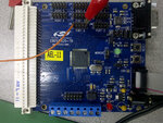
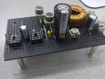
I am currently using the C8051F120 development kit (see attached) in attempt to sense the o/p voltage from my Buck convertor and adjust the PWM signal, which is also generated from the 8051 chip.

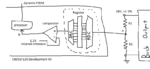
However my question is how should I connect point A (see another attachment) and interface it with the development kit?

I've read somewhere from the datasheet that there is an internal reference voltage of 1.2V and therefore I've stepped down the 28V output with a set of appropriate resistors (R1 & R2).

Assuming I would like to make about 30 samples before I made one adjustment to the PWM duty cycle, would what I've drawn in the attached been feasible?

Also, I got a hunch that I might as well omit the comparator and DAC, that is, connecting the register output directly to the processor.

Any comments would be appreciated.

Thanks in advance.

- Michael
 

Attachments

  • C8051F120.jpg
    C8051F120.jpg
    181.5 KB · Views: 83
  • C8051F120_feedback.png
    C8051F120_feedback.png
    52.7 KB · Views: 80

Ok, my objective is to get an as accurate 28V output voltage as possible. Right now, my open-loop Buck converter output is only at about 26.67V DC while "pumping" 28% duty cycle, 100kHz 3.3V PWM into my Buck.

As seen in my attached with a red circle, the input coming into the ADC0 seems like in pairs. So my question is would a single-ended input be better or a differential input to this ADC0 be more appropriate for me to obtain an as accurate 28V output as possible?

Let's say if I do not want the output voltage to exceed +/- 0.1% away from my ideal 28V, that is, assuming after stepping down to 1.2V at point A, the voltage sensed by the ADC0 must be able to detect a tiny difference of about 1.2mV (0.1% of 1.2V), would the single-ended input or the differential input configuration allow me to achieve this?

Next, I understand be it which configuration I used in the end, there would be a 8-bit register storing the ADC0 digital output after converting the analog signal. I would like to know (assuming I am using the single-ended sensing configuration, which is sensing the 1.2V directly from point A) what would the 8 bits data looks like? And also, what type of variable should I declare to capture this 8-bit data that actually represents my 1.2V for example?

Attached is my Buck converter schematic and the real photo, just in case you're interested to know what do I mean of the 28V output voltage.
 

Attachments

  • ADC0 Functional Block Diagram.jpg
    ADC0 Functional Block Diagram.jpg
    134 KB · Views: 103
  • full_sch.jpg
    full_sch.jpg
    176.9 KB · Views: 81
  • full_front.jpg
    full_front.jpg
    121.1 KB · Views: 80

Recently, I've been trying to use the sample codes: ADC and PCA (for PWM) in attempt to 1) produce a 100kHz, 28% duty cycle 3.3V PWM & 2) read an analog voltage signal in the range of 0-2.43V and display it on Hyperterminal via UART1.

Had realised that in order to create a 100kHz PWM, the CLK divider should be 0x20 and CLK multiplier should be about 0x21 to get that 100kHz, but if I change PLL0DIV = 0x20 and PLL0MUL = 0x21 accordingly, the display at the hyperterminal could not display the sensed mV properly. And if I used the default settings for PLL0DIV & PLL0MUL, the PWM will be 194kHz instead of 100kHz. So, it is really a chicken or egg problem.

Could anyone know how to do it in order for me to achieve both 1) 100kHz PWM and 2) displaying the sensed voltage correctly?

My codes are as below.

Code:
//-----------------------------------------------------------------------------
// Includes
//-----------------------------------------------------------------------------

#include <c8051f120.h>                 // SFR declarations
#include <stdio.h> 

//-----------------------------------------------------------------------------
// Global Constants
//-----------------------------------------------------------------------------

#define INTCLK       24500000          // Internal oscillator frequency in Hz
#define SYSCLK       49000000          // Output of PLL derived from (INTCLK*2)
#define BAUDRATE     115200            // Baud rate of UART in bps
#define SYSCLK       49000000          // Output of PLL derived from (INTCLK*2)
#define SAMPLE_RATE  50000             // Sample frequency in Hz
#define INT_DEC      256               // Integrate and decimate ratio
#define SAR_CLK      2500000           // Desired SAR clock speed

#define SAMPLE_DELAY 50                // Delay in ms before taking sample

sbit LED = P1^6;                       // LED='1' means ON
sbit SW1 = P3^7;                       // SW1='0' means switch pressed

//-----------------------------------------------------------------------------
// 16-bit SFR Definitions for 'F12x
//-----------------------------------------------------------------------------

sfr16 ADC0     = 0xbe;                 // ADC0 data
sfr16 RCAP2    = 0xca;                 // Timer2 capture/reload
sfr16 RCAP3    = 0xca;                 // Timer3 capture/reload
sfr16 TMR2     = 0xcc;                 // Timer2
sfr16 TMR3     = 0xcc;                 // Timer3

//-----------------------------------------------------------------------------
// Function Prototypes
//-----------------------------------------------------------------------------

void OSCILLATOR_Init (void);
void PORT_Init (void);
void PCA0_Init (void);
void Set_PCA0_Duty_Cycle(unsigned short l_us_duty_cycle);
void UART1_Init (void);
void ADC0_Init (void);
void TIMER3_Init (int counts);
void ADC0_ISR (void);
void Wait_MS (unsigned int ms);

//-----------------------------------------------------------------------------
// Global Variables
//-----------------------------------------------------------------------------

long Result;                           // ADC0 decimated value

//-----------------------------------------------------------------------------
// main() Routine
//-----------------------------------------------------------------------------

void main (void)
{
   long measurement;                   // Measured voltage in mV
   unsigned int delay_count;           // Used to implement a delay
   bit duty_direction = 0;             // 0 = Decrease; 1 = Increase

   // Disable watchdog timer
   WDTCN = 0xde;
   WDTCN = 0xad;

   PORT_Init ();                       // Initialize crossbar and GPIO
   OSCILLATOR_Init ();                 // Initialize oscillator
   PCA0_Init ();                       // Initialize PCA0
   UART1_Init ();                      // Initialize UART1
   TIMER3_Init (SYSCLK/SAMPLE_RATE);   // Initialize Timer3 to overflow at sample rate

   ADC0_Init ();                       // Init ADC

   SFRPAGE = ADC0_PAGE;
   AD0EN = 1;                          // Enable ADC

   EA = 1;                             // Enable global interrupts

   while (1)
   {
      EA = 0;                          // Disable interrupts

      // The 12-bit ADC value is averaged across INT_DEC measurements.  The result is 
      // then stored in Result, and is right-justified 
      // The measured voltage applied to AIN 0.1 is then:
      //
      //                           Vref (mV)
      //   measurement (mV) =   --------------- * Result (bits) 
      //                       (2^12)-1 (bits)

      measurement =  Result * 2430 / 4095;

      EA = 1;                          // Re-enable interrupts

      SFRPAGE = UART1_PAGE;

      printf("AIN0.1 voltage: %ld mV\n",measurement);

      SFRPAGE = CONFIG_PAGE;
      LED = ~SW1;                      // LED reflects state of switch

      Wait_MS(SAMPLE_DELAY);           // Wait 50 milliseconds before taking another sample
          Set_PCA0_Duty_Cycle(74);
   }
   
//   SFRPAGE = PCA0_PAGE;                // Change to PCA0 page
//
//   while (1)
//   {
//      Set_PCA0_Duty_Cycle(74);
//      // Wait a little while
//      for (delay_count = 30000; delay_count > 0; delay_count--);
//
//      if (duty_direction == 1)         // Direction = Increase
//      {
//         // First, check the ECOM0 bit
//         if ((PCA0CPM0 & 0x40) == 0x00)
//         {
//            PCA0CPM0 |= 0x40;          // Set ECOM0 if it is '0'
//         }
//         else                          // Increase duty cycle otherwise
//         {
//            PCA0CPH0--;                // Increase duty cycle
//
//            if (PCA0CPH0 == 0x00)
//            {
//               duty_direction = 0;     // Change direction for next time
//            }
//         }
//      }
//      else                             // Direction = Decrease
//      {
//         if (PCA0CPH0 == 0xFF)
//         {
//            PCA0CPM0 &= ~0x40;         // Clear ECOM0
//            duty_direction = 1;        // Change direction for next time
//         }
//         else
//         {
//            PCA0CPH0++;                // Decrease duty cycle
//         }
//      }
//
//   };
}


//-----------------------------------------------------------------------------
// Initialization Subroutines
//-----------------------------------------------------------------------------

//-----------------------------------------------------------------------------
// Initialization Subroutines
//-----------------------------------------------------------------------------

//-----------------------------------------------------------------------------
// OSCILLATOR_Init
//-----------------------------------------------------------------------------
//
// Return Value : None
// Parameters   : None
//
// This function initializes the system clock to use the internal oscillator
// at 24.5 MHz multiplied by two using the PLL.
//
//-----------------------------------------------------------------------------

void OSCILLATOR_Init (void)
{
   int loop;                           // Software timer

   char SFRPAGE_save = SFRPAGE;        // Save Current SFR page

   SFRPAGE = CONFIG_PAGE;              // Set SFR page

   OSCICN = 0x83;                      // Set internal oscillator to run
                                       // at its maximum frequency

   CLKSEL = 0x00;                      // Select the internal osc. as
                                       // the SYSCLK source

   //Turn on the PLL and increase the system clock by a factor of M/N = 2
   SFRPAGE = CONFIG_PAGE;

   PLL0CN  = 0x00;                     // Set internal osc. as PLL source
   SFRPAGE = LEGACY_PAGE;
   FLSCL   = 0x10;                     // Set FLASH read time for 50MHz clk
                                       // or less
   SFRPAGE = CONFIG_PAGE;
   PLL0CN |= 0x01;                     // Enable Power to PLL
   PLL0DIV = 0x01;                     // Set Pre-divide value to N (N = 1)
   PLL0FLT = 0x01;                     // Set the PLL filter register for
                                       // a reference clock from 19 - 30 MHz
                                       // and an output clock from 45 - 80 MHz
   PLL0MUL = 0x02;                     // Multiply SYSCLK by M (M = 2)

   for (loop=0; loop < 256; loop++);   // Wait at least 5us
   PLL0CN  |= 0x02;                    // Enable the PLL
   while(!(PLL0CN & 0x10));            // Wait until PLL frequency is locked
   CLKSEL  = 0x02;                     // Select PLL as SYSCLK source

   SFRPAGE = SFRPAGE_save;             // Restore SFR page
}

//-----------------------------------------------------------------------------
// PORT_Init
//-----------------------------------------------------------------------------
//
// Return Value : None
// Parameters   : None
//
// This function configures the crossbar and GPIO ports.
//
// P0.0   digital   push-pull     PCA0 CEX0
//
//-----------------------------------------------------------------------------
void PORT_Init (void)
{
   char SFRPAGE_save = SFRPAGE;         // Save Current SFR page

   SFRPAGE = CONFIG_PAGE;                 // set SFR page

    P0MDOUT   = 0x07;
    XBR0      = 0x08;
    XBR2      = 0xC4;

        // Enable UART1
        P0MDOUT |= 0x01; // Set TX1 pin to push-pull
        P1MDOUT |= 0x40; // Set P1.6(LED) to push-pull

   SFRPAGE = SFRPAGE_save; // Restore SFR page
}

//-----------------------------------------------------------------------------
// PCA0_Init
//-----------------------------------------------------------------------------
//
// Return Value : None
// Parameters   : None
//
// This function configures the PCA time base, and sets up 8-bit PWM output
// mode for Module 0 (CEX0 pin).
//
// The frequency of the PWM signal generated at the CEX0 pin is equal to the
// PCA main timebase frequency divided by 256.
//
// The PCA time base in this example is configured to use SYSCLK, and SYSCLK
// is set up to use the internal PLL running at 49 MHz.  Therefore,
// the frequency of the PWM signal will be 49 MHz / 256 = 191.4 kHz.
// Using different PCA clock sources or a different processor clock will
// result in a different frequency for the PWM signal.
//
//    -------------------------------------------------------------------------
//    How "8-Bit PWM Mode" Works:
//
//       The PCA's 8-bit PWM Mode works by setting an output pin low every
//    time the main PCA counter low byte (PCA0L) overflows, and then setting
//    the pin high whenever a specific match condition is met.
//
//    Upon a PCA0L overflow (PCA0L incrementing from 0xFF to 0x00), two things
//    happen:
//
//    1) The CEXn pin will be set low.
//    2) The contents of the PCA0CPHn register for the module are copied into
//       the PCA0CPLn register for the module.
//
//    When the PCA0L register increments and matches the PCA0CPLn register for
//    the selected module, the CEXn pin will be set high, except when the
//    ECOMn bit in PCA0CPMn is cleared to '0'.  By varying the value of the
//    PCA0CPHn register, the duty cycle of the waveform can also be varied.
//
//    When ECOMn = '1', the duty cycle of the PWM waveform is:
//
//       8-bit PWM Duty Cycle = (256 - PCA0CPLn) / 256
//
//    To set the duty cycle to 100%, a value of 0x00 should be loaded into the
//    PCA0CPHn register for the module being used (with ECOMn set to '1').
//    When the value of PCA0CPLn is equal to 0x00, the pin will never be
//    set low.
//
//    To set the duty cycle to 0%, the ECOMn bit in the PCA0CPMn register
//    should be cleared to 0.  This prevents the PCA0CPLn match from occuring,
//    which results in the pin never being set high.
//    -------------------------------------------------------------------------
//
//-----------------------------------------------------------------------------
void PCA0_Init (void)
{
   char SFRPAGE_save = SFRPAGE;        // Save current SFR Page

   SFRPAGE = PCA0_PAGE;
   // configure PCA time base; overflow interrupt disabled
   PCA0CN = 0x00;                      // Stop counter; clear all flags
   PCA0MD = 0x08;                      // Use SYSCLK as time base

   PCA0CPM0 = 0x42;                    // Module 0 = 8-bit PWM mode

   // Configure initial PWM duty cycle = 50%
   PCA0CPH0 = 256 - (256 * 0.5);

   // Start PCA counter
   CR = 1;
   SFRPAGE = SFRPAGE_save;
}

void Set_PCA0_Duty_Cycle(unsigned short l_us_duty_cycle)
{
        //Save current SFR Page
        char SFRPAGE_SAVE = SFRPAGE;

        SFRPAGE = PCA0_PAGE;

        if (l_us_duty_cycle == 0)
        {
                //For 0% duty cycle, clear ECOM0
                //PCA0CPM0 &= 0xBF;

                //lsl : 02 Jun 2011 : 1744hrs
                //For 0% duty cycle, clear ECOM0 (bit 6) & PWM0 (bit 1)
                PCA0CPM0 &= 0xBD;
        }
        else if (l_us_duty_cycle > 255)
        {
                //For 100% duty cycle
                //a. Set ECOM0 (bit 6) & PWM0 (bit 1)
                //b. Load 0x00 into PCA0CPH0

                PCA0CPM0 |= 0x42;       //0x40;

                PCA0CPH0 = 0;
        }
        else
        {
                PCA0CPM0 |= 0x42;       //0x40;

                PCA0CPH0 = 256 - (unsigned char)(l_us_duty_cycle & 0xFF);
        }

        //Restore the SFRPAGE
        SFRPAGE = SFRPAGE_SAVE;
}

void UART1_Init (void)
{
   char SFRPAGE_SAVE = SFRPAGE;        // Save Current SFR page

   SFRPAGE = UART1_PAGE;
   SCON1   = 0x10;                     // SCON1: mode 0, 8-bit UART, enable RX

   SFRPAGE = TIMER01_PAGE;
   TMOD   &= ~0xF0;
   TMOD   |=  0x20;                    // TMOD: timer 1, mode 2, 8-bit reload


   if (SYSCLK/BAUDRATE/2/256 < 1) {
      TH1 = -(SYSCLK/BAUDRATE/2);
      CKCON |= 0x10;                   // T1M = 1; SCA1:0 = xx
   } else if (SYSCLK/BAUDRATE/2/256 < 4) {
      TH1 = -(SYSCLK/BAUDRATE/2/4);
      CKCON &= ~0x13;                  // Clear all T1 related bits
      CKCON |=  0x01;                  // T1M = 0; SCA1:0 = 01
   } else if (SYSCLK/BAUDRATE/2/256 < 12) {
      TH1 = -(SYSCLK/BAUDRATE/2/12);
      CKCON &= ~0x13;                  // T1M = 0; SCA1:0 = 00
   } else {
      TH1 = -(SYSCLK/BAUDRATE/2/48);
      CKCON &= ~0x13;                  // Clear all T1 related bits
      CKCON |=  0x02;                  // T1M = 0; SCA1:0 = 10
   }

   TL1 = TH1;                          // Initialize Timer1
   TR1 = 1;                            // Start Timer1

   SFRPAGE = UART1_PAGE;
   TI1 = 1;                            // Indicate TX1 ready

   SFRPAGE = SFRPAGE_SAVE;             // Restore SFR page

}

//-----------------------------------------------------------------------------
// ADC0_Init
//-----------------------------------------------------------------------------
//
// Return Value : None
// Parameters   : None
//
// Configure ADC0 to use Timer3 overflows as conversion source, to
// generate an interrupt on conversion complete, and to use right-justified
// output mode.  Enables ADC end of conversion interrupt. Leaves ADC disabled.
//
//-----------------------------------------------------------------------------
void ADC0_Init (void)
{
   char SFRPAGE_SAVE = SFRPAGE;        // Save Current SFR page

   SFRPAGE = ADC0_PAGE;

   ADC0CN = 0x04;                      // ADC0 disabled; normal tracking
                                       // mode; ADC0 conversions are initiated
                                       // on overflow of Timer3; ADC0 data is
                                       // right-justified

   REF0CN = 0x07;                      // Enable temp sensor, on-chip VREF,
                                       // and VREF output buffer

   AMX0CF = 0x00;                      // AIN inputs are single-ended (default)

   AMX0SL = 0x01;                      // Select AIN0.1 pin as ADC mux input

   ADC0CF = (SYSCLK/SAR_CLK) << 3;     // ADC conversion clock = 2.5MHz
   ADC0CF |= 0x00;                     // PGA gain = 1 (default)

   EIE2 |= 0x02;                       // enable ADC interrupts

   SFRPAGE = SFRPAGE_SAVE;             // Restore SFR page
}

//-----------------------------------------------------------------------------
// TIMER3_Init
//-----------------------------------------------------------------------------
//
// Return Value : None
// Parameters   :
//   1)  int counts - calculated Timer overflow rate
//                    range is postive range of integer: 0 to 32767
//
// Configure Timer3 to auto-reload at interval specified by <counts> (no
// interrupt generated) using SYSCLK as its time base.
//
//-----------------------------------------------------------------------------
void TIMER3_Init (int counts)
{
   char SFRPAGE_SAVE = SFRPAGE;        // Save Current SFR page

   SFRPAGE = TMR3_PAGE;

   TMR3CN = 0x00;                      // Stop Timer3; Clear TF3;
   TMR3CF = 0x08;                      // use SYSCLK as timebase

   RCAP3   = -counts;                  // Init reload values
   TMR3    = RCAP3;                    // Set to reload immediately
   EIE2   &= ~0x01;                    // Disable Timer3 interrupts
   TR3     = 1;                        // start Timer3

   SFRPAGE = SFRPAGE_SAVE;             // Restore SFR page
}

//-----------------------------------------------------------------------------
// Interrupt Service Routines
//-----------------------------------------------------------------------------

//-----------------------------------------------------------------------------
// ADC0_ISR
//-----------------------------------------------------------------------------
//
// Here we take the ADC0 sample, add it to a running total <accumulator>, and
// decrement our local decimation counter <int_dec>.  When <int_dec> reaches
// zero, we post the decimated result in the global variable <Result>.
//
//-----------------------------------------------------------------------------
void ADC0_ISR (void) interrupt 15
{
   static unsigned int_dec=INT_DEC;    // Integrate/decimate counter
                                       // we post a new result when
                                       // int_dec = 0
   static long accumulator=0L;         // Here's where we integrate the
                                       // ADC samples

   AD0INT = 0;                         // Clear ADC conversion complete
                                       // indicator

   accumulator += ADC0;                // Read ADC value and add to running
                                       // total
   int_dec--;                          // Update decimation counter

   if (int_dec == 0)                   // If zero, then post result
   {
      int_dec = INT_DEC;               // Reset counter
      Result = accumulator >> 8;
      accumulator = 0L;                // Reset accumulator
   }
}

//-----------------------------------------------------------------------------
// Support Subroutines
//-----------------------------------------------------------------------------

//-----------------------------------------------------------------------------
// Wait_MS
//-----------------------------------------------------------------------------
//
// Return Value : None
// Parameters:
//   1) unsigned int ms - number of milliseconds of delay
//                        range is full range of integer: 0 to 65335
//
// This routine inserts a delay of <ms> milliseconds.
//
//-----------------------------------------------------------------------------
void Wait_MS(unsigned int ms)
{
   char SFRPAGE_SAVE = SFRPAGE;        // Save Current SFR page

   SFRPAGE = TMR2_PAGE;

   TMR2CN = 0x00;                      // Stop Timer3; Clear TF3;
   TMR2CF = 0x00;                      // use SYSCLK/12 as timebase

   RCAP2 = -(SYSCLK/1000/12);          // Timer 2 overflows at 1 kHz
   TMR2 = RCAP2;

   ET2 = 0;                            // Disable Timer 2 interrupts

   TR2 = 1;                            // Start Timer 2

   while(ms)
   {
      TF2 = 0;                         // Clear flag to initialize
      while(!TF2);                     // Wait until timer overflows
      ms--;                            // Decrement ms
   }

   TR2 = 0;                            // Stop Timer 2

   SFRPAGE = SFRPAGE_SAVE;             // Restore SFRPAGE
}

//-----------------------------------------------------------------------------
// End Of File
//-----------------------------------------------------------------------------
 

Status
Not open for further replies.

Similar threads

Part and Inventory Search

Welcome to EDABoard.com

Sponsor

Back
Top