Continue to Site

Welcome to EDAboard.com

Welcome to our site! EDAboard.com is an international Electronics Discussion Forum focused on EDA software, circuits, schematics, books, theory, papers, asic, pld, 8051, DSP, Network, RF, Analog Design, PCB, Service Manuals... and a whole lot more! To participate you need to register. Registration is free. Click here to register now.

how to run analysis of OP Amp(low power)

Status
Not open for further replies.

r@m$

Junior Member level 3
Joined
Jun 8, 2011
Messages
25
Helped
3
Reputation
6
Reaction score
3
Trophy points
1,283
Activity points
1,439
hi...

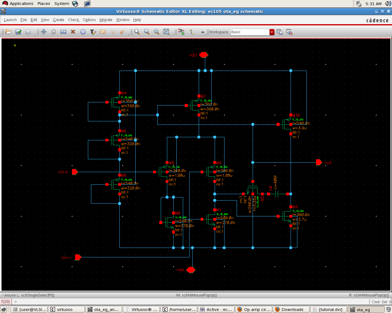
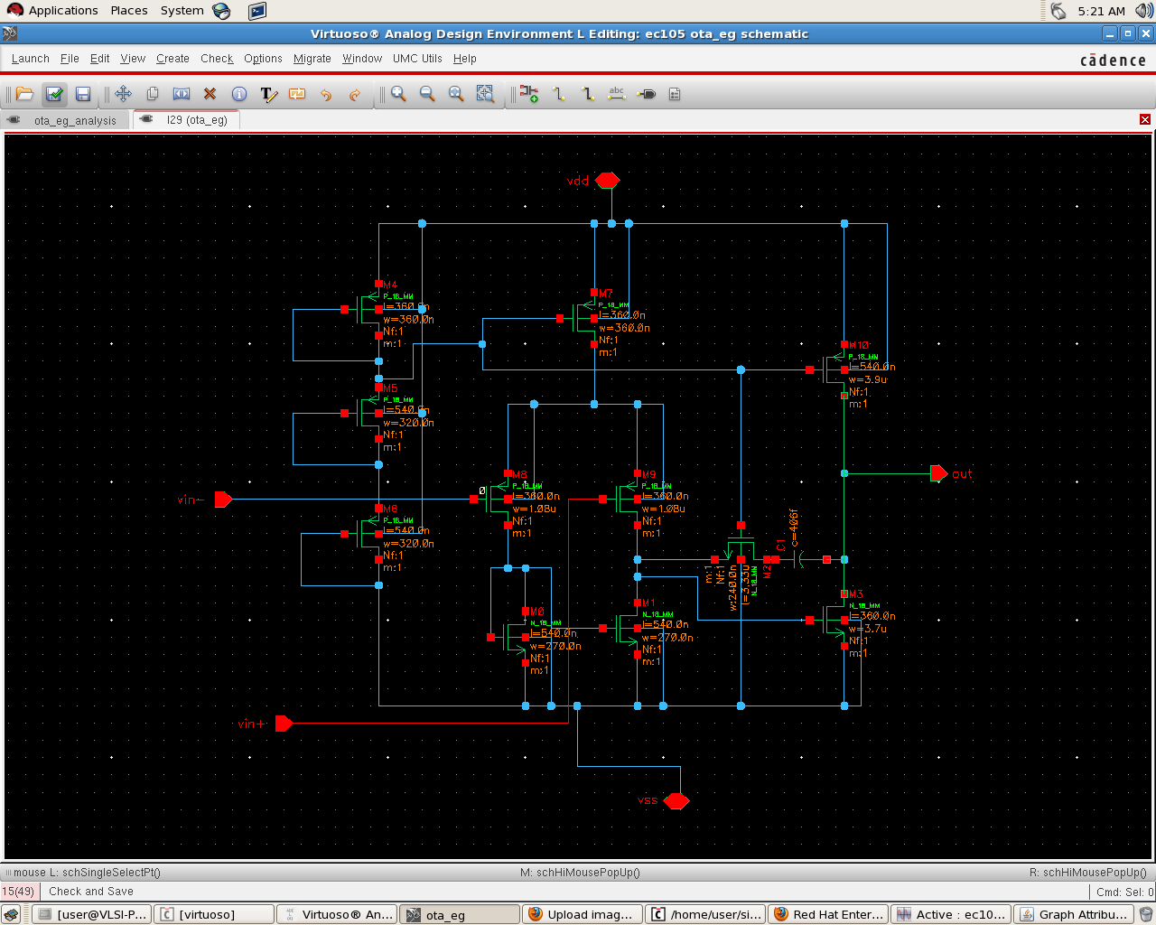
I have an op amp circuit shown in figure,,,


how can I run the ac analysis of the circuit??
i mean what are the feedback elements or any other components i need to add??


If you want only to do AC analysis, you just have to give the vdd, vss voltages by "vdc source", and add a load capacitance to the output, the voltages of vin+ and vin- can also be given by "vdc source", you only have to give ac values in the right place bisides the dc values.
 

I am getting negative gain of the order -50 dB
but i am supposed to get 75dB
 

For testing such an OTA with differential input and single output, you should know the input and output common-mode voltages for which the OTA is designed for. Also you need to design a test-bench circuit and use this OTA in a feedback loop, which sets the output common-mode voltage of the OTA based on it's input common-mode voltage. For example, if the OTA has equal input and output common-mode voltages, you can use a simple resistive negative feedback from the output of the OTA to its negative input and then apply the input signal to the positive input node of the OTA. The input signal should contain a DC value equal to the common-mode voltage of the amplifier and an ac component.
 

I am getting negative gain of the order -50 dB
but i am supposed to get 75dB

Most probably, the reason is an uncorrect bias point due to the input offset voltage.
Recommendation:
* At first, perform a dc analysis (with µV resolution between +/- 10mV) to determine the necessary input offset.
* Then, apply the corresponding dc voltage together with the ac input.
* As a result, you get the open-loop gain.
 

Also: 1- choose the resistance value as large as possible, not to affect on the OTA ac operation. 2- Use a large capacitor from the negative input of the OTA to ground, to zero the ac value of this pin.
 

hi... tanx for the reply...
am elementary in op amps design.....
how can i get the input offset voltage??
 

Hi r@m$.

I would like just notice you that in circuit you shown you have a sufficient mistake.
May be you already correct it. If not you have a wrong connection of output terminal.
May be it's a reason of unexpected simulation results.
 
  • Like
Reactions: r@m$

    r@m$

    Points: 2
    Helpful Answer Positive Rating
Agree with DenisMark! Follow the signal path!!!
 

Agree with DenisMark. This mistake might lead to wrong dc operating point and negative dc gain.
 

tanq all......
I corrected the connection of out put terminal....

But still i am getting low gain then the actual spec...

is there any other mistakes exist in my circuit????


i dont quite understand why the Vout is connecting to that point

---------- Post added at 19:08 ---------- Previous post was at 18:55 ----------

I see the new one.
Are you sure the M2 can get the correct gate voltage Vg2. I just used the poly resistance
 

tanx for the reply hsh22...

can you be more clear??
 

Hi r@m$,

even after correcting your circuit, my reply#5 ist still valid.
Since you have asked how to determine offset - it is explaine in posting#5 (dc analysis for very small input voltages with very good resolution).
 

the M2 must be biased in correct condition so the Ron can have a suitable value to eliminate the effect of the Zero .you can learn this in Razavi's book Chapter 10
 

hiii LvW...
tanx for the reply..
but i dont know how to get the input offset voltage from the dc analysis
 

hiii LvW...
tanx for the reply..
but i dont know how to get the input offset voltage from the dc analysis

The dc analysis gives the transfer characteristic around the operating point - and it crosses the zero-volt line at Voff.
 

I can't understand what do you mean by the input offset voltage!! can you explain more? What is the source of this offset?
I still think that after correcting the output node, the description in my first and second replies should be followed.
 

I can't understand what do you mean by the input offset voltage!! can you explain more? What is the source of this offset?
I still think that after correcting the output node, the description in my first and second replies should be followed.

If you work with opamps and are going to design opamps it is important to understand the relevant specifications.

In case of ideal matching of all components the opamp output (split supply assumed) should be zero for zero input voltages.
However, in reality this is not the case. The offset voltage Voff is the voltage that is necessary to apply across the input nodes to produce Vout=0 volts. The dc transfer curve crosses the zero line for a (small) input voltage that is identical to Voff (µVolts for good opamps, mVolts for universal units).
 
  • Like
Reactions: r@m$

    r@m$

    Points: 2
    Helpful Answer Positive Rating
Add Vcc source to the circuit so that you can run the amplifier.
 

Status
Not open for further replies.

Part and Inventory Search

Welcome to EDABoard.com

Sponsor

Back
Top