Continue to Site

Welcome to EDAboard.com

Welcome to our site! EDAboard.com is an international Electronics Discussion Forum focused on EDA software, circuits, schematics, books, theory, papers, asic, pld, 8051, DSP, Network, RF, Analog Design, PCB, Service Manuals... and a whole lot more! To participate you need to register. Registration is free. Click here to register now.

[SOLVED] How to reduce op amp clamp Vout to 0V?

Status
Not open for further replies.

d123

Advanced Member level 5
Joined
Jun 7, 2015
Messages
2,505
Helped
494
Reputation
992
Reaction score
525
Trophy points
1,393
Location
Spain
Activity points
27,148
Hi,

Further to the clamp circuit I asked about, I simulated it and breadboarded it today and it works as well as may be hoped/expected. I wish LEDs were more like capacitors than diodes regarding gradual turn on rather than having a Vf, anyway.

From what I'm reading and simulation and breadboard results, op amp clamps never go down to 0V, even with 0V input?

If so, is there a way of making 0V in mean 0V out? Pull-down resistors in various obvious places made no difference.

On turning the circuit on with the switch, the LEDs dimly glow before pressing the 'ON' button, and the 'OFF' button never fully turns them off, even though the charge capacitor voltage reads 5mV.

Don't mind need for switch but would be nicer with only the two pushbuttons.

Quiescent current is 2mA, housekeeping over 3mA, this is also undesirable. Is that likely to just be the components I'm using in this version?

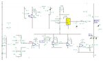
Again, sorry for drawn schematic, can't turn on laptop to do neat schematic right now. Pictures are schematic of actual circuit and same circuit on breadboard.

Thanks.

DSC_0961.JPG


DSC_0962.JPG

--- Updated ---

Hi again,

Two corrections:

1) Charge capacitor is 10uF, not 22uF.

2) I am an idiot. Quiescent current is only ~850uA. I forget to remove the green LED (top right on breadboard) when measuring total supply current...
 
Last edited:

No problem to clamp to 0 V or output 0 V from OP buffer, just need negative supply voltage for OP.

Having this said, there are ways to generate output voltage < 1 mV with single supply OPs, not sure if it's simple with LMC6464, probably yes. But you have also other options, e.g. implementing an offset in the V/I output stage.

Instead of trying to improve a given circuit, we will usually make a step back, what's the circuit purpose and specification, what's the best way to achieve it.
 
Last edited:
  • Like
Reactions: d123

    d123

    Points: 2
    Helpful Answer Positive Rating
Hi,

I usually overcome this problem the other way round.
Instead of pulling one Opamp input exactly to zero, I pull the other input slightly high.
Maybe this is what FvM already suggested.

Example: to get LED current down to zero you may add a 1k resits(or from R11/R12/R13 to U4_In-
Then add a 100k to your 1.24V reference. This gives an offset of about +12mV at U4_In-...LED current should become zero.

Klaus
 
  • Like
Reactions: d123

    d123

    Points: 2
    Helpful Answer Positive Rating
Rail-to-Rail Output The approximated output resistance of the LMC6462/4 is 180Ω sourcing, and 130Ω sinking at VS = 3V, and 110Ω sourcing and 83Ω sinking at VS = 5V. The maximum output swing can be estimated as a function of load using the calculated output resistance.

Also in spec sheet -

1600556134964.png


Whne you do your measurement where are you taking your ground reference ?
At package or somewhere in proto board. The former would be advised.


Regards, Dana.
 
  • Like
Reactions: d123

    d123

    Points: 2
    Helpful Answer Positive Rating
Hi,

Thanks for the useful solutions provided. I wanted to try out the suggestions before replying in case they led to more questions.

Choices were: two batteries for a dual supply for the op amps or TC7660 for the negative supply, or introducing an offset. Wanted simplest/smallest solution so tried Klaus' suggestion first.

I added 100k in series from LM4041 to U2 In+ and 1k in series from 'Rlimit' (R11, R12 and R13) to U4 In-. That made no difference, unfortunately, maybe I didn't understand what was suggested and did it wrong, so I added a 10k from V+ (Vsupply) to U4 In- and it has worked - there is now only ~30mV at that node but the LEDs are fully off, even connecting the battery with no on/off switch, so unless there's a reason not to do it that way, I'm content with the solution. Tried 1M, then 100k but the 10k is the only one that ensured LEDs are fully off, it adds a few hundred uA to the quiescent current so probably leave the on/off switch.

Tried powering LM4041 from PNP 'ON' button to reduce quiescent current but it seemed messy so will leave it powered all the time by the supply/battery.

I used various places as DMM ground last night, some on breadboard rail, all as close as possible to signal of interest. I have 'BI' PDIP 6464s for breadboarding and 'AI' SOIC 6464s for actual PCBs, I think you quoted AI and maybe not over temperature range as worst-case seems to be 200mV for 'BI' - I'm not disagreeing with you, Dana, as you know a lot more than I ever will, by the way. I'm 'flying blind' due to lack of electricity at present and just jot down pinouts and minimum device specifications needed to get a circuit going within device parameters, so thanks.

Now for the joy of making a sensible battery choice rather than the awful, zilch mAh 9V mini-brick for testing this idea...

Thanks a lot, guys.
 

Hi,

I've been working on this project (no simulations, just a breadboard), fwiw..., and I have got to here on the breadboard version (schematic attached) and besides many questions, I would appreciate a 'grown-up in the room' to provide some feedback about e.g.:

1a) Will a circuit like this always leak/drift to being on/white LEDs lighting up without a mechanical switch? - I suspect it will.
1b) Even on a solid ground plane on a 35um copper-clad PCB in an enclosure using only SMD parts (except for the diodes and LEDs), would a circuit like this tend to randomly turn on and/or drift to being on with no user input?

2) What is bad/naïve amateur design here, where could it be improved without too many drastic changes?

3) Will adding a buffer op amp from Node 1 to the comparator stop the slow leak charging of the C5 capacitor - without the comparator the C5 capacitor voltage doesn't rise in single mV over a minute or so or more, with the comparator IN- pin connected via a 5cm wire, it rises 1mV per second and the white LEDs turn on a bit and glow dimly in around 50 seconds after the C5 capacitor is fully discharged by the OFF (DOWN button).

4) Why won't it work with e.g an 100mV or 200mV clamp reference voltage and an 8R sense resistor (it's always on)? Why do I have to seem to need at least about 1V clamp reference and about 27R sense resistor? Surely that choice of clamp Vref should be irrelevant so long as the sense voltage is higher than the off voltage at the sense resistor (7mV) and the op amp inputs go down to ground?

5) The 100k pull-up on U4 is weak and the LEDs flash on at battery connection and disconnection, but not with a 10k - the 10k uses nearly 1mA Iq which is a huge waste/battery drain. Is there any way around this?

6) The added circuitry (comparator, Q1, 555, T5 and Q2) are intented to be on whenever the white LEDs should be on to create a duty cycle of 10% on, 90% off (my eyes can't see any flicker) to reduce current draw. I can't plug in my pathetic children's oscilloscope and am having to guess if that part of the circuit is working correctly or not by using the DMM to measure currents and voltages but am not sure it's actually working properly. I know the 10% duty cycle works by changing C22 to a 10uF capacitor and counting time between the LED 'on' flashes. Can this idea work or will adding that section just confuse the consctant current op amp and create undesired side-effects I can dimly sort of guess and wonder about?
I tried using an LMC555 reset pin to trigger when C5 capacitor was over reset pin min voltage but the results were... very bad. That is why the 555 is powered by a gating PMOS and the comparator.
7) How treacherous can a breadboard be for this circuit and play head games with me with bits that would/could work on a PCB and maybe wouldn't/couldn't on a PCB? i.e. Seem not to work ideally on a brreadboard, leakage, etc., but be nowhere near as bad on a PCB with a solid ground plane?

LEDs 4, 5, and 6 are just visual indicators, they wouldn't be on a PCB. I'm having to use a 9V battery via an adjustable regulator to emulate a battery voltage going from ~6.5V fully-charged to ~4V discharged, which I guess is also misleading as a design approach.

Sorry for so many questions. Thanks.
 

Attachments

  • Torch adjustable brightness schematic v4.JPG
    Torch adjustable brightness schematic v4.JPG
    172.4 KB · Views: 105

Hi,

1a) Will a circuit like this always leak/drift
"The circuit" won´t drift, but the battery voltage. And you connected R27 to the battery voltage, so the Opamp output will drift, too.
Thus I recommended to use the 1.2V Reference voltage instead. It should be fairly stable...

It´s not clear to me whether you mean " leak/drift to being on" as a long term drift with time and temperature or just the power_up_glitch

2) What is bad/naïve amateur design here, where could it be improved without too many drastic changes?
is the use of a tiny, low power microcontroller too drastic? .... it may reduce the part count to only 10%, maybe less. Without performance loss.

3) Will adding a buffer op amp from Node 1 to the comparator
There already is a buffer.. why don´t you use it?

5) I don´t know why you omitted the 1k resistor (Post#3)

The use of C6 is critical and may lead to oscillations.

***********
All in all I think it´s overcomplicated. But maybe I don´t understand the whole idea.

Klaus
 
  • Like
Reactions: d123

    d123

    Points: 2
    Helpful Answer Positive Rating
Hi Klaus,

Thank you.

1a) = Poor choice of words, sorry. I hadn't even considered drift with time and temperature - I meant will C5 always charge over time due to leakage from anything connected to it.
Your advice about R27 is appreciated.

2) Poverty, Klaus, poverty, it's crippling, thus my circuits made from what components I still have... I agree with you, even if I can't write MCU code, and I learn lots from analog design, a microcontroller would simplify this so much and improve it, too.

3) I thought the comparator IN- shifts when triggered so it would affect the U1 output/U2 input.

5) I'm embarrassed to admit I couldn't get that to work. I'll try again.

C6 - good point.

The circuit is designed to use C5 as an adjustable voltage reference for the constant current source op amp. So long as it can be on or off, have varying levels of brightness, and the LEDs stay fully-lit for a few minutes if needed (until C5 drains/discharges naturally), that's all it has to do.

Again, many thanks.
 

Hi,

1a) C5 will drift :-( Self discharge, leakage currents on the PCB, leakage currents by connected circuitry.

3) Connect U6_IN- to U1_out. U1_out is stable. Improves C5 performance. I see no drawback.

5) yes, try. Give feedback.

Klaus
 

    d123

    Points: 2
    Helpful Answer Positive Rating
Hi Klaus,

Hi,

1a) C5 will drift :-( Self discharge, leakage currents on the PCB, leakage currents by connected circuitry.

3) Connect U6_IN- to U1_out. U1_out is stable. Improves C5 performance. I see no drawback.

5) yes, try. Give feedback.

Klaus

1a)...So the mechanical on/off switch is obligatory to prevent spurious turn-on due to leakage charging the C5 capacitor, that's okay.

3) I tried that but it was unsuccessful so just added another op amp buffer from C5 node to U6 IN- which solved the problem.

5) Helped a bit, but adding a 100nF capacitor from Batt+ to Q1 gate has eliminated LED flash both turning SW1 on and off and when inserting the battery with the SW1 closed. Great, that flash was so annoying.

I removed C8.

__________________

To be honest, there are things I'm finding confusing about this circuit by now after this afternoon's troubleshooting and testing, which I'll put in a new post later.

Thanks a lot for your help.
 

Hi,

What's 'silly' to one person can be important to another.

I've been trying various things to remove the brief LED flash at battery connection and the LEDs dimly glowing when they should be fully off, and so as can be seen, making yet more changes to the circuit. I got rid of the pulsed section as it was no use for saving power.
A second quad op amp and PMOS is not what I'd like, but LED millisecond flash at battery connection and dimly glowing when they should be off is driving me mad as I cannot resolve these two glitches/issues. They make the circuit seem like a sub-substandard penny store product.

The latest version is this one:

PRECISION CLAMP FOR TORCH V5B.JPG


- U6 buffers the voltage reference (LM4041 on breadboard).
- U10 buffers the charge capacitor, C5, used for its high input impedance.
- U7 is being used a comparator - LM193 uses 580uA Iq on the breadboard, LMC6464 used 38uA, so even if using an op amp as a comparator is a cardinal sin, needs must. I did re-read articles about using op amps as comparators and checked the datasheet first. Iq of 180uA is something I can live with, 760uA would be a battery vampire.
- T6 is an FDC604P on the breadboard, very similar in many ways to FDS9934C PMOS - FDC604P Spice model has a temperature pin with no information about what voltage to place on it (I tried 250mV and 2.5V) and it or the FDT457N definitely freezes the simulation at 5%, so this model used here.
- T5 is an FDT457N, very similar in many ways to FDS9934C NMOS - FDT457N Spice model has a temperature pin with no information about what voltage to place on it (I tried 250mV and 2.5V) and it or the PMOS FDC604P definitely freezes the simulation at 5%, so this model used here.
- LEDS above PMOS, PMOS and NMOS in series, I know it's stupid, I did that as the PMOS gating the LEDs made no difference to my problem, either. I tried that first. The PMOS stops the LEDs dimly glowing once the battery is connected and the switch SW1 closed, despite R16 and R17.

The LEDs flash for a millisecond on connecting the battery when the switch is closed and it is really winding me up that whatever I do it won't go away. I don't want to use a switch. The second quad op amp and PMOS should be totally unnecessary.

The circuit works correctly apart from from the two infuriating glitches.

1) Can anyone think of a way of preventing this glitch?
2) Is it possible that the problem(s) is (are) caused by doing the prototyping on a breadboard, it's not the actual circuit, and on a proper PCB with a solid ground plane it wouldn't happen?

Thanks.
 

This whole design could be done on a single chip mixed signal processor, and the requisite de-
glitching handled. If I understood the inputs and their relationship to the outputs I could show
a basic design I think. Quite possibly with little or no code needed.

Alternatively a small 8 pin processor could be added to produce a delayed switch action, just using
on chip clock generation, only external component a bypass cap for the chip.

The AM inputs fed to the mirrors, whats purpose of mirrors, to sum currents into C5 ?

Regards, Dana.
 
Hi,

Did you try the 1k resistor that I recommended in post#3?


Klaus
 
Hi Klaus,

Did you try the 1k resistor that I recommended in post#3?

Yes, I did.. It's R17 (bottom right section of latest schematic). After the forum now, I'm going to try a different NMOS, see what difference - if any - it makes; maybe one with a higher VGS(th) might help.
--- Updated ---

Hi Dana,

This whole design could be done on a single chip mixed signal processor, and the requisite de-
glitching handled. If I understood the inputs and their relationship to the outputs I could show
a basic design I think. Quite possibly with little or no code needed.

Alternatively a small 8 pin processor could be added to produce a delayed switch action, just using
on chip clock generation, only external component a bypass cap for the chip.

The AM inputs fed to the mirrors, whats purpose of mirrors, to sum currents into C5 ?

Regards, Dana.

Okay, that would be interesting to see, but bear in mind money is very, very tight so I wouldn't be able to implement your design, only learn from it. My only coding experience is making an LED turn on and off in Python with a Raspberry Pi-style device. If you want to share the idea, great, if not, great.

The current source and sinks charge C5, which acts as a variable voltage reference for the op amp constant current source to vary brightness. After 1V to ~V+, the C5 discharge rate makes LEDs stay on x time without further button pressing.
 
Last edited:

Hi,

R17 should not be connected to GND, but to the upper pin of R10 as feedback path (instead of the fix wire).

Test if it works to get LED current down to zero.

The next step is to use a 1uF ... up to 10uF from U4_1 to U4_2 to suppress the "power up flash".

Klaus
 
Hi,

Okay, I'll eventually put the 1k in the right place...

Thanks.
 

So you have an up & dwn input to raise or lower LED brightness.

Then if no button is being pressed the led brightness ramps down over a fixed time,
from what it was after buttons were no longer being pressed.

I understand the current source. What is the top sig chain doing U10 thru T6, I see the
same V from C5 thats being fed to the LED current driver is going to the upper sig chain.
What is that for ?

Range of LED current needed ? Time C5 discharges to turn LEDs completely off ?


Regards, Dana.
 

Hi,

... Finally got rid of glitchy flash on connecting battery and dim glow. Placing R17 as suggested helped, adding 1uF as suggested also helped but tiny flash persisted. Changed FDT457N (VGSth max. 3V) for ZVN4206A (VGSth max. 4.5V) and flash completely gone.

So, have been able to remove extra quad op amp and PMOS - hooray. Iq still 180uA as LM4041 needed more current to have stable 1.220 to 1.223V from 0mA to 25mA.

Maybe I cooked the FDT457N a bit soldering it to homebrew adapter board (I had to do it outdoors in midday heat on a block of wood on a concrete flower box..)or static-damaged it when tracing the tracks around it on the PCB, no idea if it's damaged or not - basic test of pushbutton and LED prior to use was normal, i.e. functionally correct.

Reduced Vref for current sense to 0.5V, Rsense to 20R to accommodate much higher RDS(on) of ZVN4206A. Circuit now functions correctly from 3.9V to 6.5V with 25mA out max at both ends. ...Even if I know no battery has/4*AA batteries in series have much current left when drained so far (see this new post by dick_freebird in this thread on that topic), the adjustable regulator and 9V battery are best I can do to emulate 4*AA typical life.

Thanks Klaus, solved the flaws in the circuit.
--- Updated ---

Hi Dana,

So you have an up & dwn input to raise or lower LED brightness.

Then if no button is being pressed the led brightness ramps down over a fixed time,
from what it was after buttons were no longer being pressed.

That's correct.


I understand the current source. What is the top sig chain doing U10 thru T6, I see the
same V from C5 thats being fed to the LED current driver is going to the upper sig chain.
What is that for ?

That monstrosity was throwing components at a circuit out of desperation and ignorance about how to solve two problems - ignore it. I have removed that part as it is no longer needed.

Range of LED current needed ? Time C5 discharges to turn LEDs completely off ?

0mA to ~25mA max.
Not an especially fixed amount of time, a few minutes will do, the point is not to have to keep pressing the 'up' button every 30 seconds to have a few or 10 minutes light.

Best mention, I might change C5 from 47uF to 220uF for longer fully-on duration until it falls below Vclamp (~510mV) and eventually drains to nothing, so in analog would to try to add fast charge and fast discharge buttons with slow charge and slow discharge buttons by switching in and out two different source/sink resistors, seems easy on paper..., if it's too hard to implement real-world without endless problems I'm happy with the current version - basically, the schematic in post #1.
 
Last edited:

Status
Not open for further replies.

Part and Inventory Search

Welcome to EDABoard.com

Sponsor

Back
Top