Continue to Site

Welcome to EDAboard.com

Welcome to our site! EDAboard.com is an international Electronics Discussion Forum focused on EDA software, circuits, schematics, books, theory, papers, asic, pld, 8051, DSP, Network, RF, Analog Design, PCB, Service Manuals... and a whole lot more! To participate you need to register. Registration is free. Click here to register now.

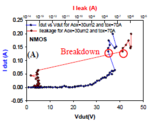
How to read this I-V characteristic curve which represents the device breakdown

Status
Not open for further replies.

junsik

Junior Member level 2
Joined
Feb 17, 2015
Messages
23
Helped
0
Reputation
0
Reaction score
0
Trophy points
1
Activity points
207
캡처.PNG


I'm reading a paper,

Malobabic, S.; Ellis, D.F.; Salcedo, J.A.; Yuanzhong Zhou; Hajjar, J.-J.; Liou, J.J., "Gate oxide evaluation under very fast transmission line pulse (VFTLP) CDM-type stress," Devices, Circuits and Systems, 2008. ICCDCS 2008. 7th International Caribbean Conference on , vol., no., pp.1,8, 28-30 April 2008
doi: 10.1109/ICCDCS.2008.4542669

In this paper, the uploaded graph is contained to check the NMOS gate oxide breakdown point by ESD stress.

I have some problem to read the graph. Please tell me the way to read the graph. or some information the graph. what is it called?
 

In this graph see the change of current when the voltage is increasing
the region 5v to 40v current is almost linear
 

Status
Not open for further replies.

Similar threads

Part and Inventory Search

Welcome to EDABoard.com

Sponsor

Back
Top