ssankurathri
Full Member level 3
Hi,
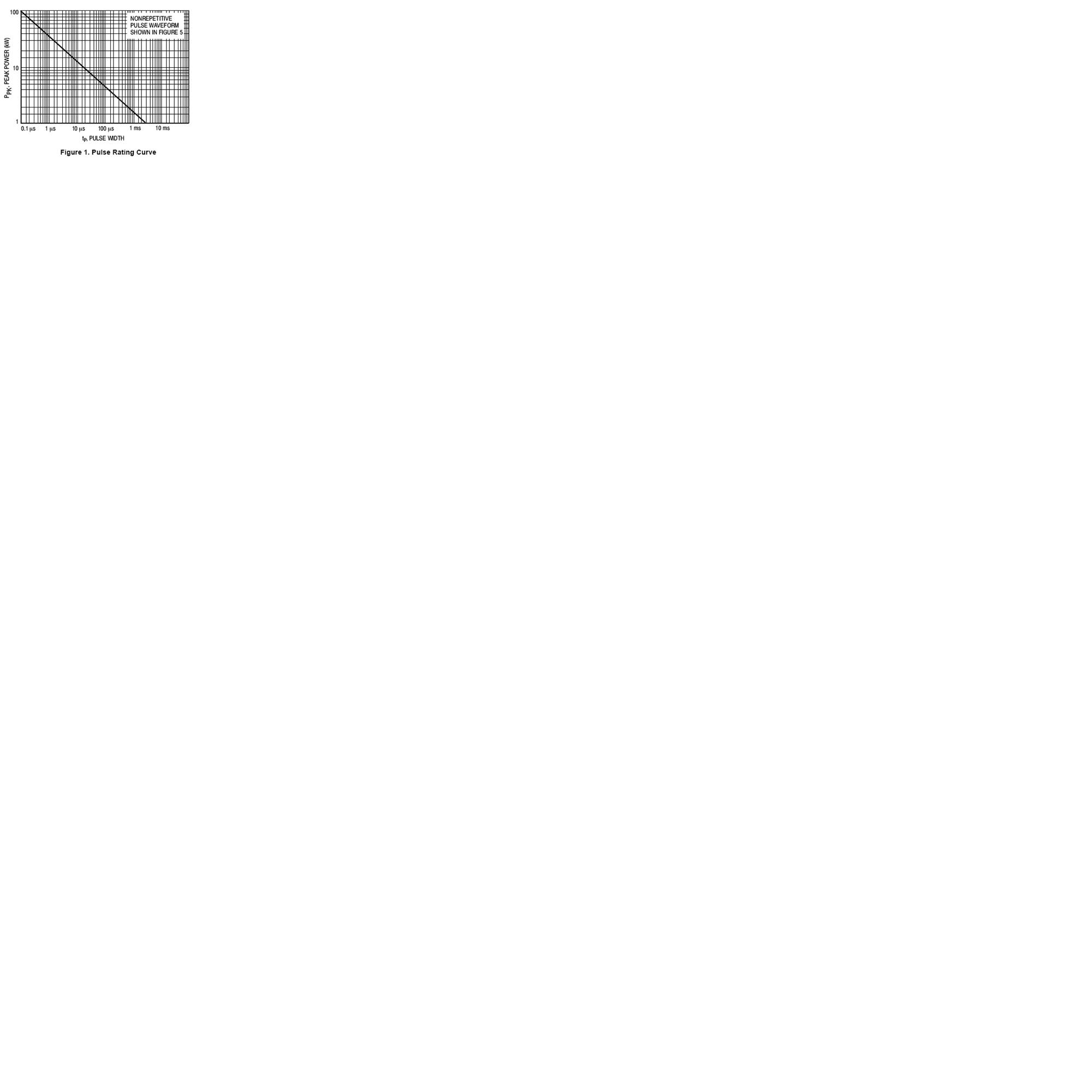
these are zener diode power dissipation characteristics. how to read this graph and come up with the selection of proper zener for application?

these are zener diode power dissipation characteristics. how to read this graph and come up with the selection of proper zener for application?