Continue to Site

Welcome to EDAboard.com

Welcome to our site! EDAboard.com is an international Electronics Discussion Forum focused on EDA software, circuits, schematics, books, theory, papers, asic, pld, 8051, DSP, Network, RF, Analog Design, PCB, Service Manuals... and a whole lot more! To participate you need to register. Registration is free. Click here to register now.

[SOLVED] How to protect my MosFETs???

Status
Not open for further replies.

faraj

Member level 1
Joined
Feb 22, 2005
Messages
40
Helped
1
Reputation
2
Reaction score
1
Trophy points
1,288
Location
Azarbaijan/ Tabriz
Activity points
1,601
hi everyone,

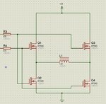
i'm working on a circuit in which i want to apply pulses to an inductive load. to produce pulses i'm using Power MosFET (IRF840). as the load is inductive i want to protect the mosfet against reverse current or what is so called. but my problem is that i'm applying pulses to the load in both directions not just one direction and in order to do this i'm using 4 mosfets to feed 1 load so i don't know where to put the protective circuit. i attach the circuit, i think it is much better than describing :). first, i'll apply positive pulse (right-to-left) then a after an interruption i'll apply the negative pulse (left-to-right).

thank you in advance for your time and effort.
 

Attachments

  • Inductive Load.jpg
    Inductive Load.jpg
    113.8 KB · Views: 164

Hi,
Your circuit is a classic H Bridge. You need to put in high speed schottky diodes in parallel with the mosfets.
This link should be helpful : **broken link removed**

Cheers,
Scanman
 
  • Like
Reactions: faraj

    faraj

    Points: 2
    Helpful Answer Positive Rating
And don't forget the dead time in your control unit (software or hardware) between the half cycles to give enough time for the coil to discharge almost completely (through the added 4 diodes on the H-bridge, actually through 2 diodes after each half cycle),

On the other hand, please try to test your circuit first using a resistance load (not too light or too heavy) instead, to see what you will get on it (I mean its voltage). For this test you likely don't need the 4 diodes.

By the way, I didn't check yet the datasheet of your MOSFET... perhaps it has also its reverse diode (between Drain and Source).

Kerim

Added:
IRF840 has already an internal diode... I think you don't need to add one externally.
Please don't forget the test with a resistive load (simulation or real).
 
Last edited:
  • Like
Reactions: faraj

    faraj

    Points: 2
    Helpful Answer Positive Rating
Your gate drive really needs to change - it is just a bit too simplistic, the reverse diodes in the mosfets will protect the devices - a decent cap on the main bus will help here too - as will tight layout of the H bridge, your dead time between lower and upper devices on each half bridge need only bee 200nS or greater - regards, Orson Cart.
 
  • Like
Reactions: faraj

    faraj

    Points: 2
    Helpful Answer Positive Rating
If you intend to drive the high side mosfet gates with 5v it will not work at all.
If you try to use a Nmosfet as a high side switch and you drive the gate with the same voltage (or lower) that you apply to the drain then the mosfet will be in a half open state, depending on the gate threshold of the mosfet you will have an increased Vds voltage drop over the mosfet.

To use the high side N mosfets correctly you have to apply to the gate a voltage that is higher then the drain, this happens because when the mosfet turns on the source voltage will be almost equal to the drain (for example 10v), if you have applied that same 10v to the gate then you suddenly have no Vgs bias and this creates the problem.

You also have to separate the gates of the upper and lower mosfets because the upper ones will need a voltage ab about 32v and at this voltage the lower side mosfets will be damaged.

Alex
 
  • Like
Reactions: faraj

    faraj

    Points: 2
    Helpful Answer Positive Rating
Hi Alex... That is why I have suggested him to simulate (or build with a resistive load just in case) his circuit first :smile:

Only then he will understand much better what you liked him to know.

My best learnings happened after my failures. :grin:

Kerim
 
Last edited:
  • Like
Reactions: faraj

    faraj

    Points: 2
    Helpful Answer Positive Rating
Thank you everyone for your suggestions and helps. KerimF is right there are 2 type of IRF840 and one (IRPOWER) has internal protection diode so it doesn't need extra protection. and Alexan_e is right the circuit needed some changes in order to work propely. now i changed the circuit and it works perfectly in simulation and i think it would work in real. here i attach the new circuit to the post. thanks again.
 

Attachments

  • Inductive Load1.jpg
    Inductive Load1.jpg
    183.4 KB · Views: 164

Just a minor remark:
Aren't R1 and R3 parallel? The same is for R2 and R4.
 
Last edited:

I think you would still have problems because you can't apply any dead-time, you control each side of the bridge with one transistor that turns on the high mosfet or the low mosfet.
In order to apply deadtime you have to turn off the mosfet , use a small delay (becasue mosfets don't turn off intimidate) and then turn on the other mosfet of the same side, this way you can make sure that you don't have both mosfets of the same side conducting.

You have also done another mistake for which I have warned you in my previous post, you apply to the lower side mosfets a gate voltage of 24V but the absolute max according to the datasheet is 20V so they will be damaged.

Alex
 

Hi Alex... I wonder how he didn't notice the surge current at each transition.

Added:
It happens that when I got, at last, a good result on one side, I forgot to check out what is happening also on some other sides :oops:
 
Last edited:

Hello Faray, what kind of logic for driving of those mosfets will you use? Because when the inductive load is driving in only one direction the null diode has to be connected paralell to the inductive load and in reverse direction. It's because you don't want to interrupt current flow through the load (when the mosfet is turned off, the current flow is closed through the null diode) and so the inductive load will not produce voltages spikes. I think that is important to drive by PWM signal only high side mosfet (for example) and low side mosfet has to be open in all time in appropriate direction. In this case the diodes must be on the both low side mosfets as it is in your scheme. The current flow then will not be interrupted during the low level of PWM signal, the current flow will be closed through the one of the diode on low side mosfet and through the second still opened (in appropriate direction) mosfet on the other side. I have never build this kind of circuit but i studied it, because i will need to build such one, so appeal to some experts, tell us: is it right what did i write?
 

Just a minor remark:
Aren't R1 and R3 parallel? The same is for R2 and R4.

yes, you are right, i did not notice at first and then i removed the 1k resistors and the simulation result was the same.

---------- Post added at 06:54 ---------- Previous post was at 06:49 ----------

i use a PIC16F876 PWM output to drive the transistors. indeed i just simulated the circuit and everything was fine in simulation and now i am going to build a prototype and test it then i'll be able to share the real test results with you.
 

now i am going to build a prototype and test it then i'll be able to share the real test results with you
I you are implementing the circuit from post #7 and operating it with a 24V supply, be sure to have a sufficient stock of replacement transistors. They are likely to be blown immediately. Alexan_e has clearly told why. Alternatively, you should look out for a circuit that drives the gates in a non-overlapping way, also keeping the specified maximum vaoltage ratings. I'm sure that some have been posted at edaboard before.
 

I you are implementing the circuit from post #7 and operating it with a 24V supply, be sure to have a sufficient stock of replacement transistors. They are likely to be blown immediately. Alexan_e has clearly told why. Alternatively, you should look out for a circuit that drives the gates in a non-overlapping way, also keeping the specified maximum vaoltage ratings. I'm sure that some have been posted at edaboard before.

what if i use 12 VDC supply instead of 24 VDC? because i have both options and if this circuit would work with no problem with 12 VDC i prefer to use 12 volt.
 

You have to provide a Vgs of at least 5v to turn the mosfets on but to get the best Rds-on you need a Vgs of about 10-12v.

The lower side mosfet Vgs is referenced to gnd so if you apply 12v to the gate the Vgs will be 12v, the bridge power supply level doesn't make a difference for them.

For the high side mosfets the gates are referenced to the (mosfet) source which will have the same voltage as the drain when the mosfet is on so depending on the power supply of the mosfets you need a Vsupply+12v (assuming non isolated sources) if you want to apply a 12v Vgs.
If you use a 12v power supply for the bridge then you can use 12v to the gates of the lower mosfets to turn them on and 24v to the gates of the upper mosfets to turn them on with a Vgs of 12v.

Alex

P.S. I have changed the solved status of the thread, this is clearly not solved yet

EDIT: ignore post, it applies to the four mosfet bridge only
 

Hi Alex... I noticed he replaced the upper ones with p-channel MOSFET on the pic of post #7 so he needs only to refine how to drive the gates if he uses only 12V as supply... this is what I saw through my glasses :-?
 

i also found another configuration of the H-Bridge and simulated it in Proteus with 12 VDC can you please take a look at this one and give your opinion. it seems to me that this one is more better than the previous one.
 

Attachments

  • Inductive Load2.jpg
    Inductive Load2.jpg
    173.7 KB · Views: 137

Hi Alex... I noticed he replaced the upper ones with p-channel MOSFET on the pic of post #7 so he needs only to refine how to drive the gates if he uses only 12V as supply... this is what I saw through my glasses :-?

yes in the second circuit and also the last circuit there is a combination of P-channel and N-channel mosfets.
 

First, I guess the internal diode of the IRF840 is much more effective than 1N4001... so you can remove D3 and D4 (same for D1 and D2).

Second, as you said, since the load is inductive there will be a lagging current after the turn off of one leg and which will continue to flow for a short time in the upper and lower diodes (of the opposite leg). You need to calculate or better to measure this extra on time of the load. You can do that on the real circuit by letting the dead time between two half cycles rather wide. Then you will decide on how much short it can be (obviously you may like to leave a generous margin :smile: ).

Third, if the MOSFET models are good enough and the power dissipation of the upper P-MOS is reasonable then the rather high value of R5 and R6 may not need to be lowered (these two resistors determine the slope of the turn off current).

Any question? :grin:

Kerim

Added:
I suppose that behind R10 and R9 there is a rail-to-rail output.
 
Last edited:

Hi Alex... I noticed he replaced the upper ones with p-channel MOSFET on the pic of post #7 so he needs only to refine how to drive the gates if he uses only 12V as supply... this is what I saw through my glasses :-?

Yes you are right, I'm obviously not as good as my PC in multitasking (doing two thing at the same time).
Ignore my post, it applies only to the four Nmosfet version.

Alex
 

Status
Not open for further replies.

Similar threads

Part and Inventory Search

Welcome to EDABoard.com

Sponsor

Back
Top