Continue to Site

Welcome to EDAboard.com

Welcome to our site! EDAboard.com is an international Electronics Discussion Forum focused on EDA software, circuits, schematics, books, theory, papers, asic, pld, 8051, DSP, Network, RF, Analog Design, PCB, Service Manuals... and a whole lot more! To participate you need to register. Registration is free. Click here to register now.

how to model a photodiode in a simulation

Status
Not open for further replies.

mightyocean

Newbie level 6
Joined
Mar 18, 2006
Messages
13
Helped
0
Reputation
0
Reaction score
0
Trophy points
1,281
Activity points
1,378
reverse bias photodiode spice model

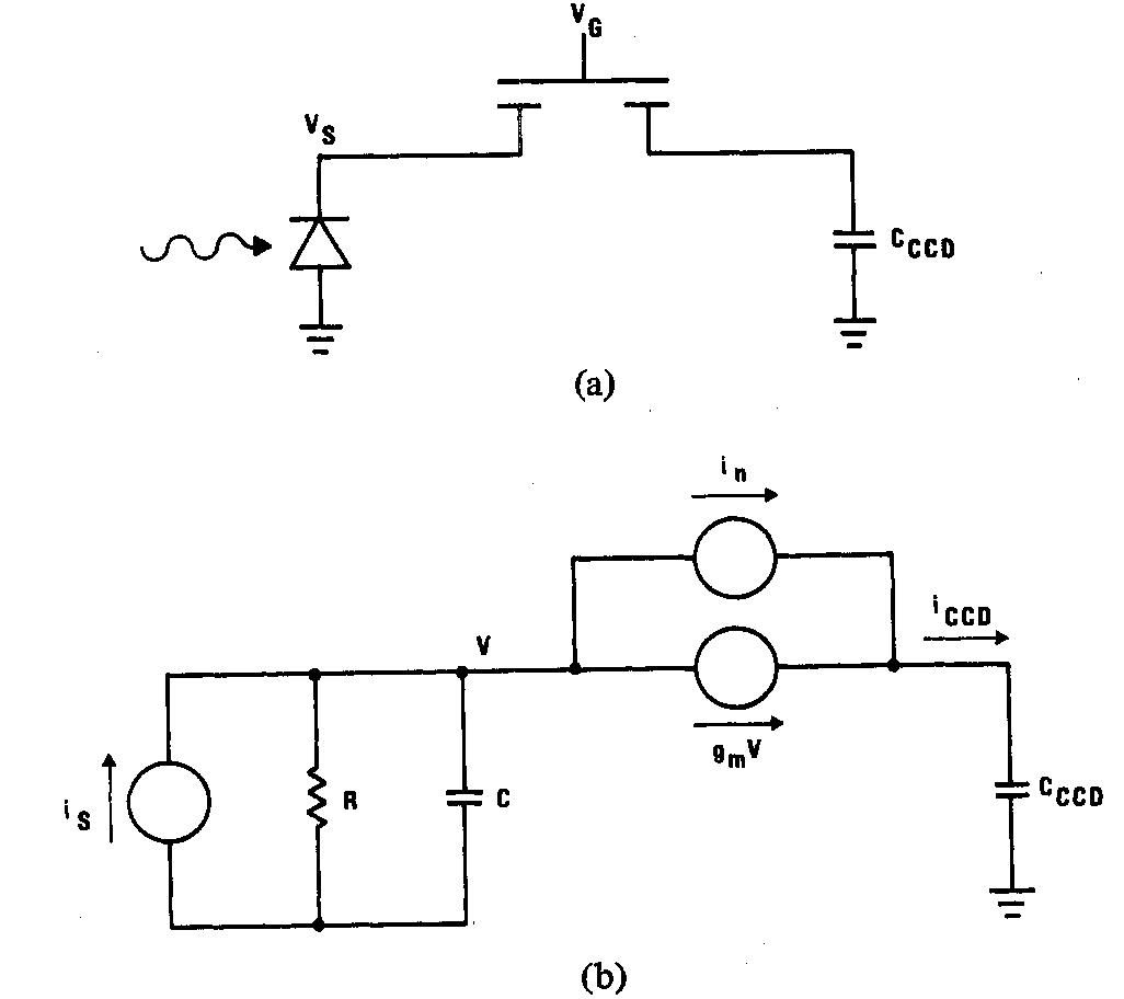
a photodiode is a part of active pixel sensor circuit, it can generate a current and inject into a MOS source, how can I model its resistance and capcitance, to set a appropriate voltage for MOS?
 

photodiode parallel with capacitor

I'm not sure what you're wanting.

If you want to model a photodiode, then you have to describe it with equations. There is modelling software available to help you create models.

The photodiode doesn't actually generate a current, photons absorbed by the silicon excite electron-hole pairs. These hole-pairs will recombine rapidly unless trapped by something. The junction of a reverse-biased diode traps (seperates) the electron hole pairs, this is the photocurrent.

The capacitance of a diode varies with voltage also.

If on the other hand you want to simulate an APS in SPECTRE or spice etc., just add a current source from gnd to the head of the diode.
 

spice modelling reverse biased photodiodes

hi Old Nick

picture (a) is the configuration and picture (b) is the equivalent circuit, the diode is modeled as a current source with its resistance and capacitance, the MOS is modeled as a VCCS, my goal is to decide the W/L of the MOS transistor. As you referred, the parameters of reversed-bias diode is varied with different photocurrent, and the source/drain voltages of MOS vary too.
but the Is*R is not large enough for the MOS transitor to operate in the weak inversion region. By the way, my diode is reverse biased at 5V.
I want to know how to configure the diode model circuit and the MOS transitor properly to bias the MOS transitor and run a simulation in spectre.
Thank you.


reverse bias photodiode

Hi
The equivalent model of Photodiode is: A current source parallel with a capacitor.
so, the current source is variable (by the incident light in the photodiode).
The capacitor Cd is equal to value Cd=10fF par example.
 
photodiode spice

hi Cesar92,
you mean set the value of the capacitor in the property table?
par means what?


Cesar92 said:
Hi
The equivalent model of Photodiode is: A current source parallel with a capacitor.
so, the current source is variable (by the incident light in the photodiode).
The capacitor Cd is equal to value Cd=10fF par example.
 

Cesar92 said:
Hi
The equivalent model of Photodiode is: A current source parallel with a capacitor.
so, the current source is variable (by the incident light in the photodiode).
The capacitor Cd is equal to value Cd=10fF par example.

A very poor model!

From 3.3V to 0V the capacitance of a diode will vary by over 100%.

mightyocean:

Just sim it in Cadence, or whatever you're using. Don't use an equivalent model circuit for your sim though, it will be very innacurate. Just sim it using the diode with the model supplied by the foundry, this will be very-very accurate.

The sort of equivalent circuit you're talking about is for simple hand calculations.

Attach a current source between gnd and point Vs then sim. Trust me, I design these things for a living!
 

HI,nick

the photodiode I use is not the Si based, so there is no model for me and I need a equivalent circuit to approch its behavior, I only know the zero bias current and resistance,what should I do then?
thanks
 

Cd=10fF, it's just an example for cadence sim.
 

mightyocean said:
HI,nick

the photodiode I use is not the Si based, so there is no model for me and I need a equivalent circuit to approch its behavior, I only know the zero bias current and resistance,what should I do then?
thanks

What is it then, I'm familiar with most devices available in most processes.

How can you expect someone to answer a question on how to model a device when you do not tell them what device you're working with?
 

Hello everyone,

I'm getting familiar with photodiodes modeling since it is the topic of my internship.
I guess you want an accurate model at inverse bias voltage...
Well, in this case it has been demonstrated lately that the reverse current depends on the voltage (thus creating a dynamic parallel resistance). The current can be due to several macanisms : diffusion, band to band tuneling, trap assisted tuneling.
It has been shown that the increase of the current with the reverse bias voltage can be model using a current gain coeficient (M = 1 + 2^(2(V-Vth)/Vth) with Vth = 6,8*Eg). At very low reverse bias votlage a parameter should be added to take into acount the field dependance on bias voltage.
Then the dynamic resitance can be easily dedued calculating the slope (R(V)=(Vd(i)-Vd(I+1))/((Id(i)-Id(I+1)).

Last, it's worth knowing that the M coefficient accounts for avalanche phenomenon, consequently according to the quality of the photodiode M accounts for the reverse current for a variable range of bias voltage. In case the diode is badly desined and fabricated the leaking current becomes prevaling at certain bias voltage.
 

Status
Not open for further replies.

Part and Inventory Search

Welcome to EDABoard.com

Sponsor

Back
Top