unbuildpain
Full Member level 2
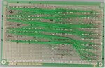
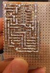
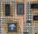
I have a blunt soldering rod, it is like that from the time I got, I was trying make project I found on YouTube, in that video the person made the traces on perforated board using solder, I tried doing that but when I dragged the solder and soldering rod, I couldn't make traces, the solder was sticking around the holes and covering the holes.