Continue to Site

Welcome to EDAboard.com

Welcome to our site! EDAboard.com is an international Electronics Discussion Forum focused on EDA software, circuits, schematics, books, theory, papers, asic, pld, 8051, DSP, Network, RF, Analog Design, PCB, Service Manuals... and a whole lot more! To participate you need to register. Registration is free. Click here to register now.

How to make the Inversion Coefficient (IC) fixed?

Status
Not open for further replies.

melkord

Full Member level 3
Joined
May 18, 2018
Messages
151
Helped
0
Reputation
0
Reaction score
1
Trophy points
18
Activity points
1,767
I am reading the book by Binkley in order to characterize my device by using Inversion Coefficient method.
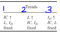
This is from Table 4.1 from the book.
1628616196237.png


What setup should I used to get IC constant?
The constant IC is used in Trend #2 and #3
I have checked other sources about Inversion Coefficient like, this and this and this, but I am still confuse how to extract the parameters, i.e., what to sweep? what to be fixed?.

Previously, I used gm/Id method.
This is similar with Trend #1 in the picture above.
I sweep VGS. VDS is half VDD. Width is fixed. L is varied for 5 different values.
It works well to extract gm, fT, but not gds.
I need gds information to be able to do the design exploration from the small signal analysis.

If you have any tutorial or other references how to properly setup the circuit to extract those parameter, I would like to know.
 

gds depends on ID, L, VDS. If VDS is fixed, you can "estimate" gds and the actual will depend on VDS.
The current depends on VGS much more than VDS. This is why in gm/ID, the VDS is fixed because it has a secondary effect (if the device is well in saturation).
If you want a good gds in gm/ID, try to estimate how much your VDS will be and set your VDS in testbench to it. An important note is that you have to have VDS= V* or more to avoid much dependency on VDS. If your V*=0.2 V, VDS=0.3V or 0.4 V will result in closer gds values. But if you have VDS=0.15 V, you will end up with much smaller gds.
Hi...I am sorry I cannot understand your hint clearly.
Could you explain more how I can characterize gds pretty accurately?
 

Hi...I am sorry I cannot understand your hint clearly.
Could you explain more how I can characterize gds pretty accurately?
You draw your circuit. try to estimate how the voltage headroom will be distributed and accordingly how will VDS be on each device.
Then put this VDS in your tesbench to generate gm/ID charts. This would give you a close value to the actual gds. Of course if you set VDS to a small value, you have to generate the charts at a limited range of VGS to have the transistor in saturation.
But again, the purpose of the charts is not to give exact values. It is to give a good starting point for choosing W.
May I ask why do you want very accurate gds? Do you get much less gds in actual circuit? If this is the case, the transistor is not deep enough in saturation. You have to make it a bit deeper into saturation.
 

You draw your circuit. try to estimate how the voltage headroom will be distributed and accordingly how will VDS be on each device.
Then put this VDS in your tesbench to generate gm/ID charts. This would give you a close value to the actual gds. Of course if you set VDS to a small value, you have to generate the charts at a limited range of VGS to have the transistor in saturation.
hmmm...so you are suggesting me to characterize one device with its terminal voltages close to the ones when this device is used in the real circuit?
If you are, I depend on simulation too much and I have to do this every time I want to get pretty accurate gds.
I am trying to avoid that.

But again, the purpose of the charts is not to give exact values. It is to give a good starting point for choosing W.
May I ask why do you want very accurate gds? Do you get much less gds in actual circuit? If this is the case, the transistor is not deep enough in saturation. You have to make it a bit deeper into saturation.
I would like to have gds information in order to be able to plug gds values into my small signal formulas derived by hand calculation.
I wonder why every characterization tutorial never takes a look into characterizing gds while I think this is as important as gm and fT. This also makes me wonder if I might have been understanding this incorrectly.
Obtaining gm values alone is not enough to be able to make use of our hand calculation formulas.
Only that one by Binkley that mentioned about characterizing gds, but I need to make IC constant during characterization. That is what I asked in my original post.
How different is your actual gds from the characterised one? is is like you get 1/2 the gds in characterisation or something 80%?
The reason is that gds is not characterised very accurate because the designer can change VGS, VDS, VSB but VDS of secondary importance if you are "well in saturation" and VSB effect is also less. If you take VDS and VSB alos into account, then you end up with a large matrix where you lose your control. So it was seen that design plays with the most important parameters VGS choose L based on the requirement of gds with a reasonable accuracy. You can have a 3D matrix (VGS, VDS, L) with sweeping VDS also but then you lose the original idea of having intuitive design starting point.
sorry for late response...i need to do something else.
Today I come across this problem again that I need gds information.

The results are very different, as expected according to Binkley's book. It is so different that I dont use gds vs gm/Id plot anymore from my current method, i.e., trend#1 in my original post.

Yes, I read one book about characterizing the technology with Matlab and later we have large matrix and can call back all the information we need by giving size or biasing. It is a great book. But I consider my self as beginner so I want to have some methods that I can use on paper as a starting point.
 
Last edited:

In your 1st link shows only dependence on Vds , one might assume maximum power transfer (MPT) is when load matches Zout but necessarily true for optimization. This good lecture article explains a lot of common FET theory and future implementations incl, varactors, spiral inductors and more specifically achieving maximum Q of the gate with independent control of body voltage Vsb which is the basic function of a PN junction's varactor C*Rp product and effect on maximum dissipation quality factor Q = Omega*CRp and how that affects Vt and Cg vs Vb. Including some processes not in use.


Not read your other links yet.

more fundamentals FWIW https://instruct.uwo.ca/engin-sc/ece370a/ECE_9706/LectureSlides/Lec04.pdf


Just change Lec0x file name for all series


Chapter 7.2 on GBW
 
Last edited:
Status
Not open for further replies.

Part and Inventory Search

Welcome to EDABoard.com

Sponsor

Back
Top