Continue to Site

Welcome to EDAboard.com

Welcome to our site! EDAboard.com is an international Electronics Discussion Forum focused on EDA software, circuits, schematics, books, theory, papers, asic, pld, 8051, DSP, Network, RF, Analog Design, PCB, Service Manuals... and a whole lot more! To participate you need to register. Registration is free. Click here to register now.

[SOLVED] How to link output of PLL to ODDR2?

Status
Not open for further replies.

kenleigh

Member level 1
Joined
Jan 3, 2011
Messages
36
Helped
1
Reputation
2
Reaction score
1
Trophy points
1,288
Activity points
1,525
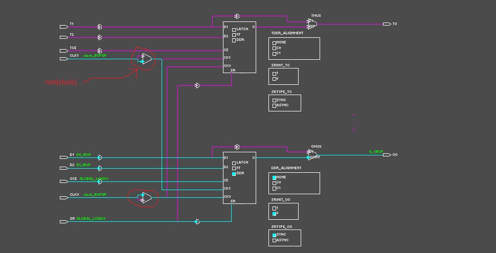
My top level module looks like this

Code:
module clkgenerator
( CLK_INP1, CLK_OUTP1, RST, LOCD);
 
  input CLK_INP1, RST;
  output CLK_OUTP1, LOCD;

// INST_TAG
  clk_wiz_v1_5 camclk
   (// Clock in ports
    .CLK_IN1            (CLK_INP1),    // IN
    // Clock out ports
    .CLK_OUT1           (CLK_OUTP1),    // OUT
    // Status and control signals
    .RESET              (RST),        // IN
    .LOCKED             (LOCD));      // OUT
// INST_TAG_END

endmodule

Now I have to add a ODDR2 to the output. But I don't know how to link the clk output of the pll CLK_OUTP1 to the input of the ODDR2.

I think I would instantiate a ODDR2 like this

Code:
	ODDR2 
	#(
	.DDR_ALIGNMENT("NONE"), // Sets output alignment to "NONE", "C0" or "C1"
	.INIT(1'b0), // Sets initial state of the Q output to 1’b0 or 1’b1
	.SRTYPE("SYNC") // Specifies "SYNC" or "ASYNC" set/reset
	) ODDR2_inst (
	.Q(//What to fill in here), // 1-bit DDR output data  
	.C0(//What to fill in here), // 1-bit clock input
	.C1(//What to fill in here), // 1-bit clock input
	.CE(1'b1), // 1-bit clock enable input
	.D0(1'b1), // 1-bit data input (associated with C0)
	.D1(1'b0), // 1-bit data input (associated with C1)
	.R(1'b0), // 1-bit reset input
	.S(1'b0) // 1-bit set input
);


But as you can so I have no idea of what to fill in .Q, .C0 and .C1
 

C1 C0 are clock inputs, Q is data output, rising edge C0 D0 appear on Q, rising edge C1 D1 appear on Q, DDR
 

Do I have to add a not gate at the input of the ODDR2?
 

Yes you can, code not(c1) will not add LUT, fpga will use another means. below these is snapshot from FPGA editor
 
Thank you for the answer and the uploaded snapshot however I'm sorry I did not understand what you intend to show me using that?

should I modify my code like this

in the PLL instantiation I will change

Code:
 .CLK_OUT1           (clkout_buf)

I would add a not gate also

Code:
not not1(clkout_buf_n ,clkout_buf);

Then in the ODDR inst I will do
Code:
ODDR2_inst (
	.Q(CLK_OUTP1), // This would be my final output
	.C0(clkout_buf), // 1-bit clock input
	.C1(clkout_buf_n), // 1-bit clock input

You said we can achieve this even without a not gate, how can we do that?
 

I am using vhdl,

ODDR2_inst : ODDR2
generic map (
DDR_ALIGNMENT => "NONE",
INIT => '0',
SRTYPE => "SYNC")
port map (
Q => Q, -- 1-bit DDR output data
C0 => clock, <---------- clock is your signal from PLL
C1 => not(clock), <------- not clock, inverting clock signal from PLL, synthesizer will not tell you about gated clock, because he will use that MUX from IO block
D0 => D0, -- 1-bit data input (associated with C1)
D1 => D1 -- 1-bit data input (associated with C1)
);
 
Thanks for the help. I will figure out the equivalent in Verilog.
Many Thanks!
 

You can do:

Code:
ODDR2_inst (
    .Q(CLK_OUTP1), // This would be my final output
    .C0(clk),      // 1-bit clock input
    .C1(~clk),     // 1-bit clock input
    // the rest...

For example on a spartan-6 this negate will be absorbed into the ODDR2. The screenshot shows you that the C0 and C1 both have the capability to negate the incoming clock. So like kirill said, you do not need an additional LUT or flipflop to generate the negated clock.
 
Status
Not open for further replies.

Part and Inventory Search

Welcome to EDABoard.com

Sponsor

Back
Top