Continue to Site

Welcome to EDAboard.com

Welcome to our site! EDAboard.com is an international Electronics Discussion Forum focused on EDA software, circuits, schematics, books, theory, papers, asic, pld, 8051, DSP, Network, RF, Analog Design, PCB, Service Manuals... and a whole lot more! To participate you need to register. Registration is free. Click here to register now.

How to improve the open loop gain for a single-ended op amp

Status
Not open for further replies.

jane_miemie

Newbie level 2
Joined
Oct 22, 2013
Messages
2
Helped
0
Reputation
0
Reaction score
0
Trophy points
1
Activity points
22
Hi everyone,

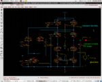
I'm new to op amp design. I've finished designing a single-ended folded cascode op amp but the open loop gain is fairly low. I'm not sure whether I set up the open loop gain configuration wrong or not. Another problem is now the output resistance is very high, can anybody give me an idea how to lower it? NEED HELP!!! Thanks a lot!!!

I'm using TSMC 0.2um and the specifications I use are listed below:
Vthn = 0.38V Kn = Un*Cox = 226.4uA/V^2
Vthp = -0.422V Kp = Up*Cox = 100.4uA/V^2
Vdd = 2.5V
CL = 10pF
slew rate = 10V/us
output voltage: min = 0.5V max = 2V
input CM voltage: min = 1V max = 2.5V
power dissipation < 5mW
Av > 60dB
GB = 10MHz
schematic.pngac_response.png
 

Hi,

An op-amp's gain is directionally proportional to Current... so by mirroring exactly ... you can achieve good Gain...

And also Every technology has a Appropriate length for exact current mirroring.. for example tsmc40 has minimum length of "700nm" to mirror exact current....(i dont know for this pdk)..

And increase the area of the differential pair you used.. You are using "200nm" length.. just increase it..

Then i have made small corrections to the schematic you uploaded... In this schematic,.. if you reduce the Bottom N_MOS pair's "vdsat" the gain will increase...
And make good sizings of the cascode pair,....

If you need swing means use CS stage... its optional...

and 10pF load cap looks just a bit high...

Try and let me know the results...

Please see the schematic..

Thanks
 

Attachments

  • schematic.png
    schematic.png
    85.5 KB · Views: 100

Thank you for your reply kenambo! Since it's a given course project, I can't change the topology now. But those specifications are chosen by myself. Since I have no experience in designing op amp, I feel I may not make good choices of the specifications. The goal here is to design a general purpose op amp and use general specifications. But I'm not sure the values I set are normal or not. Do you think Vdd = 2.5V is too low? Then how about slew rate? Is it better to make slew rate larger?
 

....

And also Every technology has a Appropriate length for exact current mirroring.. for example tsmc40 has minimum length of "700nm" to mirror exact current....(i dont know for this pdk)..

...

Hi there, can you explain more in details about the sentence I quote from your reply? I'm very interested.

Thanks in adv.
regard
Mirro
 

Thank you for your reply kenambo! Since it's a given course project, I can't change the topology now. But those specifications are chosen by myself. Since I have no experience in designing op amp, I feel I may not make good choices of the specifications. The goal here is to design a general purpose op amp and use general specifications. But I'm not sure the values I set are normal or not. Do you think Vdd = 2.5V is too low? Then how about slew rate? Is it better to make slew rate larger?

Hi,
We can make operate this topology..

No problem with supply voltage..
And regarding slew rate... i think your load cap is a bit higher try 1pF...

and Slew rate directly proportional to CURRENT....

If you need better slew rate means you have to inject more current into the cap...

for example... V= (I * T)/C--> this is simple calc to get the current for required slew rate... i.e (V/T) = I/C so ur cap is 10p then you need 100uA current to be injected into the cap... so, Try CL = 1p...

Then, Coming to gain section....

1) Increase the "length" of all devices above "500n" for good current mirroring...

2)Then increase the width of the Differential pair... and if necessary, add more multipliers.. to increase the "Gm" of the differential pair.. It also decides overall gain...
3)Then increase width of "N6" and multipliers to bias more current in differential pair...

4)In the cascode stage, Make the top(P1,P2 moses) pmos pair's width is somewhat higher,, because its going to source more current ...

5)Bottom nmos pairs ([N0,N1] [N2,N3]) sizes should be less than top Pmos pairs...

Then, make sure all the moses are in "saturation region" .. IIt is important for high gain..
I think these steps will help you...

In short, increase the current in your circuit,... this will automatically gives high gain..

Hope this will help you.. search the net for some pdfs.. docs..

Let me know if you have doubts..

Thanks...

- - - Updated - - -

Hi there, can you explain more in details about the sentence I quote from your reply? I'm very interested.

Thanks in adv.
regard
Mirro

Hi,

good to see your interest..

Curent mirroring...is greatly depends on Channel length of MOSes.... Because "Leff" will vary for various lenght Mosfets... So that for current mirroring we just change the width to get mirroring..

So for a technology, Biasing greatly depends on current mirroring.. its important to choose length which causes reduced variations...
So before starting current mirror design.. we choose "length" for which the "Vds" and "Id" variation is smaller...

It is important ot reduce the effect of "CHANNEL length modulation" parameter... which cause non-linearities in mirroring

Thats what i mentiond there..

Thanks..
 

Thanks for your reply.
Considering 'Channel length modulation', does it mean that the length is wider, the better matching in current mirroring can be always obtained?
regard,
Mirro
 

1. Keep Higher lengths for your load devices to get better Ro for your Op-Amp.
2.Reduce current in the folded stage to get higher Ro.
3.Increase Widths of Input pair and keep min lengths to get higher GM.
4.Increase tail current in the input pair stage to increase Gm.

Gain = Gm * Ro.

The Folded Cascode topology gives the advantage that we can individually play with Gm and Ro.

Can you use an actual Bias circuit rather than using voltage sources? Then you will not have to change the bias voltages for every minor change that you do.
 

Thanks for your reply.
Considering 'Channel length modulation', does it mean that the length is wider, the better matching in current mirroring can be always obtained?
regard,
Mirro

hi,
yes of course... length should be somewaht higher to reduce the effects of channel length modulation... not so high... By doing this the difference between "vds" and "Id" is very less in the operating conditon which we call as good mirroring..

Thanks..
 

Status
Not open for further replies.

Part and Inventory Search

Welcome to EDABoard.com

Sponsor

Back
Top