Continue to Site

Welcome to EDAboard.com

Welcome to our site! EDAboard.com is an international Electronics Discussion Forum focused on EDA software, circuits, schematics, books, theory, papers, asic, pld, 8051, DSP, Network, RF, Analog Design, PCB, Service Manuals... and a whole lot more! To participate you need to register. Registration is free. Click here to register now.

How to improve the bandwidth of this PTAT circuit by frequency compensation

Status
Not open for further replies.

bhl777

Full Member level 6
Joined
Sep 30, 2008
Messages
363
Helped
0
Reputation
0
Reaction score
0
Trophy points
1,296
Activity points
5,140
Hi All, I am using the circuit from this paper in designing a PTAT circuit
"A Novel Wide-Temperature-Range, 3.9 ppm/C CMOS Bandgap Reference Circuit",by changing the input transistor of opamp from MOSFET to BJT.

This is the PTAT circuit and the detailed schematic of Opamp. Startup circuit is not included in this figure.
CIRCUIT.JPG

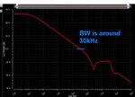
When I did the stability analysis in Cadence, by injecting IPROB at the output node of opamp, I got this bode plot
BW.JPG

As this figure shows, I tried to put a cap in A node and another one in B node, but they does not help in increasing the BW.
STB_NODE.JPG
(1) I do not know if my IPROB location is correct or not.The purpose of this BW increment is to deal with high Slew rate VCC raising, eg,1us from 0V to 2.5V.
(2) if it is correct, could anyone tell me where I can try to put the cap or RC to increase the bandwidth?
(3) if the iprobe injection is not correct for the preparation of start up, could anyone show me how to do the frequency compensation? I tried to inject the IPROB in the path of current mirror to negative input side of opamp, but the low frequency gain is 0dB and higher frequency gain is smaller, it seems like that is not a right way to probe the bandwidth of this PTAT circuit.

Thank you!
 
Last edited:

Hi,
The IPROB location is correct, you are breaking the loop at the symetric point.
But all the compensation you do will reduce the BW of the loop to achieve stability. So, you can try to push the complex poles away and reduce the compensation. But its a simple 2 stage loop and I'm not sure why you get complex poles less than a decade. I guess the bode plot you have plotted is for Cap at B, trying to introduce a Zero in the loop?
 

Hi yuvan,

Thank you for your advise! The bode plot I got is automatically generated from Cadence, after I put the iprobe at that place. So I do not know if this bode plot is for B node or anywhere.
Could you tell me how can I introduce a zero in this loop?

Hi,
The IPROB location is correct, you are breaking the loop at the symetric point.
But all the compensation you do will reduce the BW of the loop to achieve stability. So, you can try to push the complex poles away and reduce the compensation. But its a simple 2 stage loop and I'm not sure why you get complex poles less than a decade. I guess the bode plot you have plotted is for Cap at B, trying to introduce a Zero in the loop?
 

No I was asking if the BOde plot was simulated with the comp cap at node B? I was thinking introducing a CAp at node B will eventually look like a Zero WRT to loop gain. (Differencing impedance iincreases)
 

How does the current probe measure the loop gain? Which ratio do you define as loop gain?
 

No I was asking if the BOde plot was simulated with the comp cap at node B? I was thinking introducing a CAp at node B will eventually look like a Zero WRT to loop gain. (Differencing impedance iincreases)


Yes the simulation was with a 1fF cap in node B. It seems like adding the cap there does not help and no additional zero is found by adding that cap. Do you have any other suggestion in adding the zero?

At the mean time, can we say, if BW cannot be improved, this PTAT will oscillate when fast VCC is applied?

Thank you!
 

The compensation cap connected @ node B is 1fF? If so that seems to be too low to see any effect @ 30MHz BW.
 

Could you also produce the phase plot?
At the mean time, can we say, if BW cannot be improved, this PTAT will oscillate when fast VCC is applied?
Why do you think that the circuit will oscillate? When doing the tran simulation, did you confirm that the circuit oscilated?


BR Jerry
 
Last edited:

When doing the tran sim, if the SR is big enough, the output current is not a DC level but look like sine wave, although the amplitude is not big. Besides, it is very time consuming for the simulator in plotting that kind of curve.
Could you also produce the phase plot?

Why do you think that the circuit will oscillate? When doing the tran simulation, did you confirm that the circuit oscilated?


BR Jerry

- - - Updated - - -

The compensation cap connected @ node B is 1fF? If so that seems to be too low to see any effect @ 30MHz BW.

Thank you yuvan, I found the low BW was caused by low bias current, and in that case, compensation does not help anymore. Thanks for your help!


Hi All,

Generally, in Band-gap references we do insert a small "ac signal" in between output of Op-Amp & gate terminals of PMOS transistors, for analyzing stability, right?

As we know, output of Op-Amp is the low impedance node.
What ever the small ac signal we are applying will go into the output of Op-Amp as it is low impedance node. What ever the signal we apply has to pass through the loop for analysis purpose, which is not happening in this case, right? Then how can we analyze the stability?

Could any one help me in understanding this?

Thank you.

regards,
Subhash C
 

No, opamp output is not (generally) low impedance & it's the loop which makes it low impedance. So, when you are breaking the loop the output of the amp is no longer low impedance & so Stability analysis will give proper results.


"No, opamp output is not (generally) low impedance & it's the loop which makes it low impedance"

Could you please elaborate your explanation on above sentence?

thanks!
 

Status
Not open for further replies.

Part and Inventory Search

Welcome to EDABoard.com

Sponsor

Back
Top